Compound semiconductors and their application

Active Publication Date: 2013-01-10
LG CHEM LTD
View PDF1 Cites 1 Cited by
  • Summary
  • Abstract
  • Description
  • Claims
  • Application Information

AI Technical Summary

Benefits of technology

[0029]According to the present disclosure, a new compound semiconductor material is provided.
[0030]In one aspect, the new compound semiconductor may replace a conventional compound semiconductor or may be used as another material in addition to the conventional compound semiconductor.
[0031]Further, in one aspect of the present disclosure, since the compound semiconductor has good thermoelectric conversion performance, it may be used for a thermoelectric conversion device. In particular, the compound semiconductor according to the present d

Problems solved by technology

However, many conventional compound semiconducto

Method used


Image

  • Compound semiconductors and their application
  • Compound semiconductors and their application

Examples


Example

Example

[0065]In, Co, Sb and Te were prepared as reagents, and were mixed by using mortar to prepare a mixture with a composition of In0.25Co3.88Sb11Te in a pellet form. The materials mixed as above were put into a silica tube and vacuum-sealed and then heated at 650° C. for 36 hours. The time for raising the temperature to 650° C. was 1 hour and 30 minutes, and In0.25Co3.88Sb11Te powder was obtained.

[0066]A part of the composed materials prepared above was formed into a cylinder having a diameter of 4 mm and a length of 15 mm. After that, a pressure of 200 MPa was applied thereto by using a CIP (Cold Isostatic Pressing). Subsequently, the obtained result was put into a quartz tube and vacuum-sintered for 12 hours.

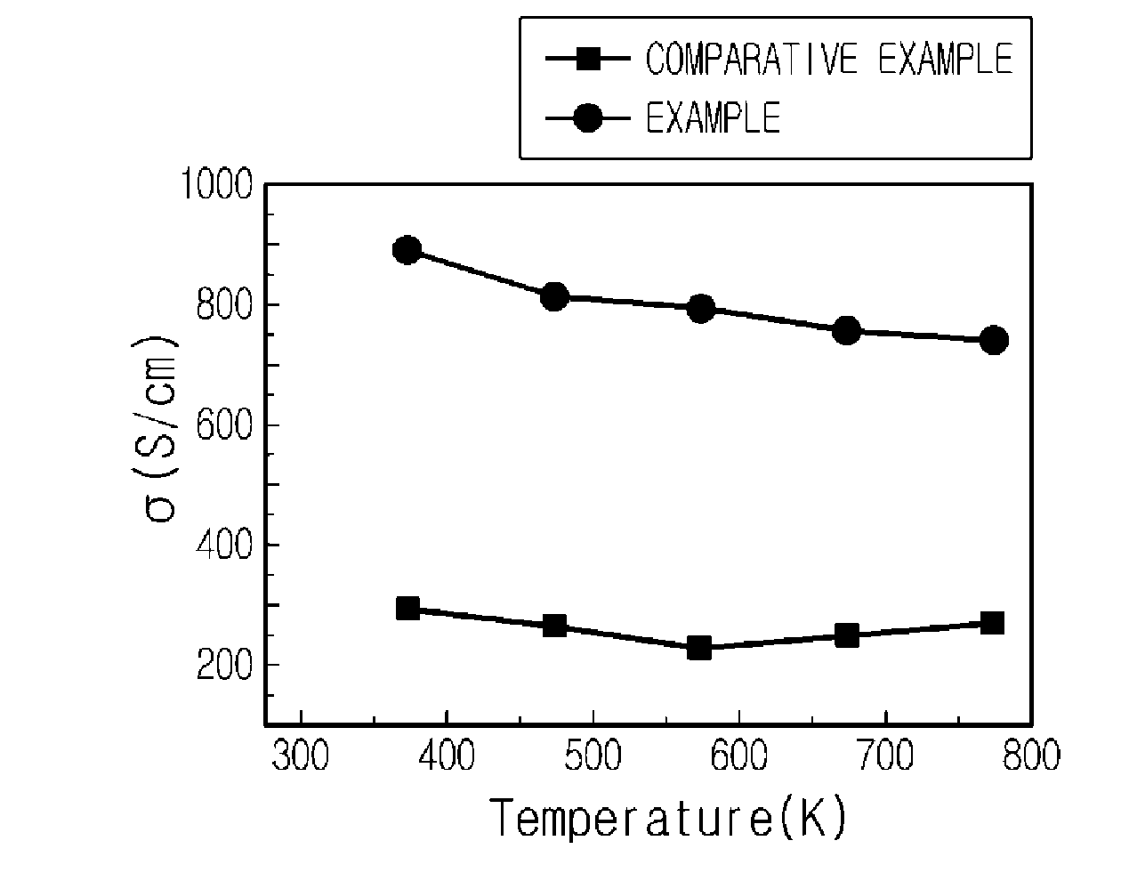
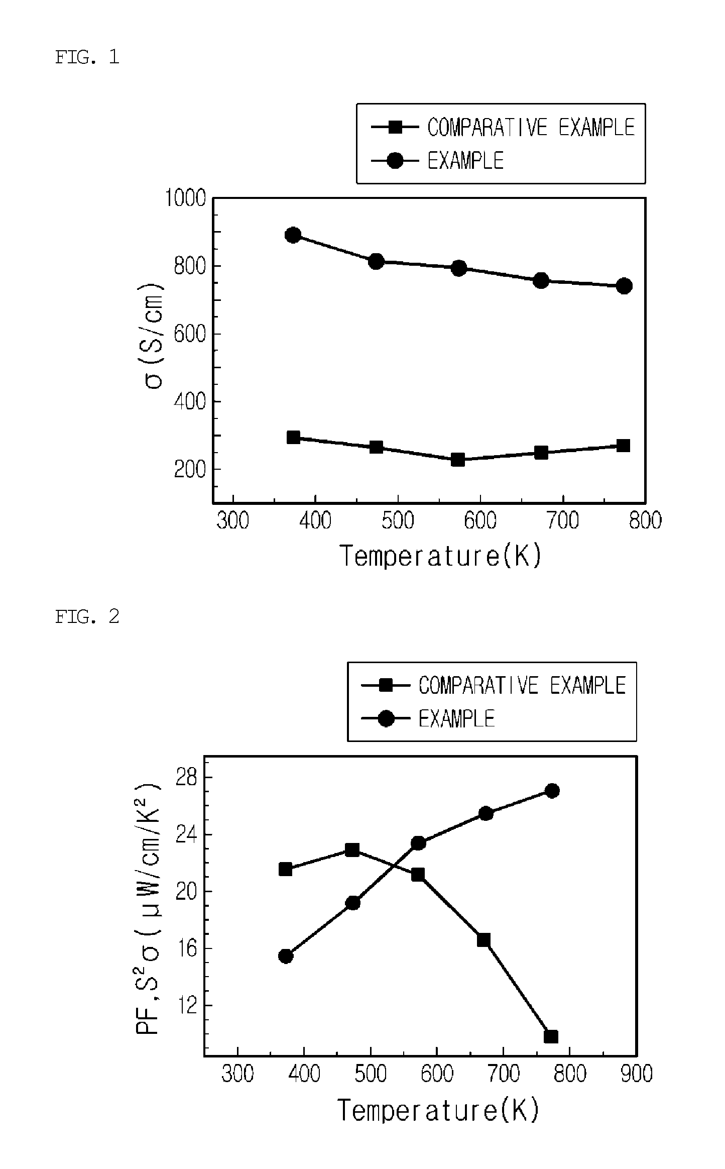
[0067]In regard to the sintered cylinder, electric conductivity (σ) was measured by using ZEM-3 (Ulvac-Rico, Inc) at predetermined temperature intervals. The measurement result is shown in FIG. 1 as the Example. In addition, a Seebeck coefficient (S) was measured by using Z...


PUM


Abstract

Disclosed are new compound semiconductors which may be used for solar cells or as thermoelectric materials, and their application. The compound semiconductor may be represented by a chemical formula: InxCo4-aSb12-zQz, where Q is at least one selected from the group consisting of O, S, Se and Te, 0<x≦0.5, 0<a≦1 and 0≦z≦4.

Description

CROSS-REFERENCE TO RELATED APPLICATION[0001]This application is a continuation of International Application No. PCT / KR2012 / 003726 filed on May 11, 2012, which claims priority to Korean Patent Application No. 10-2011-0045348 filed on May 13, 2011, Korean Patent Application No. 10-2011-0045349 filed on May 13, 2011, Korean Patent Application No. 10-2011-0049609 filed on May 25, 2011 and Korean Patent Application No. 10-2012-0050260 filed on May 11, 2012 in the Republic of Korea, the entire contents of which are incorporated herein by reference.TECHNICAL FIELD[0002]The present disclosure relates to a new compound semiconductor material which may be used for solar cells or as thermoelectric materials, its preparation method, and its applications.BACKGROUND ART[0003]A compound semiconductor is not a single element such as silicon and germanium but a compound having two or more kinds of combined elements serving as a semiconductor. Various kinds of compound semiconductors have been develo...

Claims


Application Information

Patent Timeline
IPC IPC(8): H01B1/06H01B1/10H01B1/08C01B19/00C01G15/00C01G51/00H01L31/042
CPCC01G51/006C01B19/002C01P2002/50C01P2006/32C01P2006/40C01G55/002H01L31/032H01L21/02565H01L21/02568H01L21/02614C01G53/006H01L35/18H10N10/853C07F11/00C07F15/06C07F9/90C07F5/00
Inventor PARK, CHEOL-HEEKIM, TAE-HOON
Owner LG CHEM LTD
Why Eureka
Try Eureka