Novel compound semiconductor and usage for same

A compound and semiconductor technology is applied in the field of new compound semiconductor materials to achieve good thermoelectric conversion performance and increase the ZT value.

Active Publication Date: 2014-01-15
LG CHEM LTD
View PDF7 Cites 2 Cited by
  • Summary
  • Abstract
  • Description
  • Claims
  • Application Information

AI Technical Summary

Problems solved by technology

However, many conventional compound semiconductors cannot satisfy all these conditions simultaneously

Method used


Image

  • Novel compound semiconductor and usage for same

Examples


Embodiment

[0059] Prepare 0.0510g In, 0.3873g Co, 2.2923g Sb, 0.0428g Co 3 o 4 and 127.6 g Te as a reagent and mixed using a mortar. The material mixed as above was put into a quartz tube and vacuum-sealed, then heated at 650 °C for 36 hours. The time taken to raise the temperature to 650°C was 1 hour and 30 minutes, and In 0.25 co 4 Sb 10.6 o 0.4 Te powder.

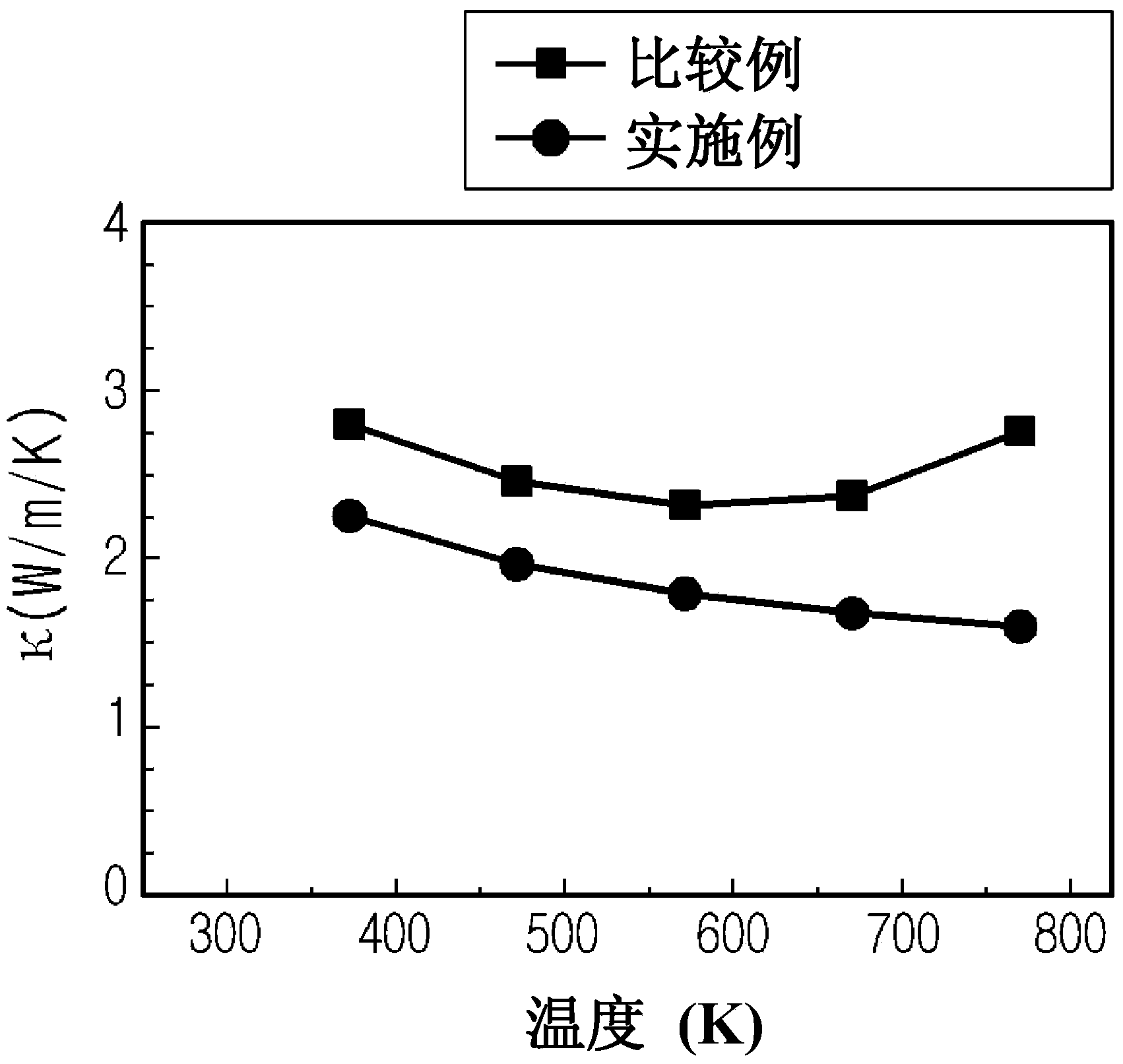
[0060] Part of the composite material produced above was formed into a disk having a diameter of 10 mm and a thickness of 1 mm. Thereafter, a pressure of 200 MPa was applied to the disk using CIP (cold isostatic pressing). Next, the resulting product was put into a quartz tube and vacuum sintered for 12 hours. For the sintered discs, thermal conductivity was measured at pre-set temperature intervals using an LFA457 (Netzsch, Inc). The measurement results are shown as examples in figure 1 middle.


PUM

PropertyMeasurementUnit
thicknessaaaaaaaaaa

Abstract

The present invention discloses a novel compound semiconductor for use in a solar cell or as a thermoelectric material, among others, and a usage for same. The compound semiconductor according to the present invention can be represented by following chemical formula 1. [Chemical formula 1] InxCo4Sb12-n-zQ'nTez, wherein in the chemical formula 1, Q' is at least one element selected from a group consisting of O, S, and Se, and x is more than 0 and less than or equal to 0.5,n is more than 0 and less than or equal to 2, and z is more than 0 and less than or equal to 2.

Description

technical field [0001] The present disclosure relates to a novel compound semiconductor material that can be used in solar cells or as a thermoelectric material, as well as the preparation method and use of the material. [0002] This application claims Korean Patent Application No. 10-2011-0045348 filed on May 13, 2011 in Korea, Korean Patent Application No. 10-2011-0045349 filed on May 13, 2011, filed in May 2011 Priority of Korean Patent Application No. 10-2011-0049609 filed on May 25 and Korean Patent Application No. 10-2012-0050459 filed on May 11, 2012, the entire contents of which are incorporated herein by reference middle. Background technique [0003] A compound semiconductor is not a single element such as silicon and germanium, but a compound containing two or more composite elements serving as semiconductors. Various compound semiconductors have been developed and used in many fields. For example, compound semiconductors can be used in thermoelectric conversi...

Claims


Application Information

Patent Timeline
Patent Type & Authority Applications(China)
IPC IPC(8): C01B19/00C01G15/00C01G51/00C01G30/00H01L31/042
CPCC01G51/006C01B19/002Y02E10/541Y02P70/50H10N10/853C07F11/00C07F3/00C07F15/06C07F9/90
Inventor 朴哲凞金兑训
Owner LG CHEM LTD
Why Eureka
Try Eureka