Thermoelectric conversion device, and cooling method and power generating method using the device
A thermoelectric conversion device and thermoelectric conversion technology, which are applied in the manufacture/processing of thermoelectric devices, thermoelectric devices, circuits, etc., can solve the problem of not reaching the thermoelectric conversion performance index, etc., and achieve the effect of excellent thermoelectric conversion performance.
- Summary
- Abstract
- Description
- Claims
- Application Information
AI Technical Summary
Problems solved by technology
Method used
Image
Examples
Embodiment approach 1
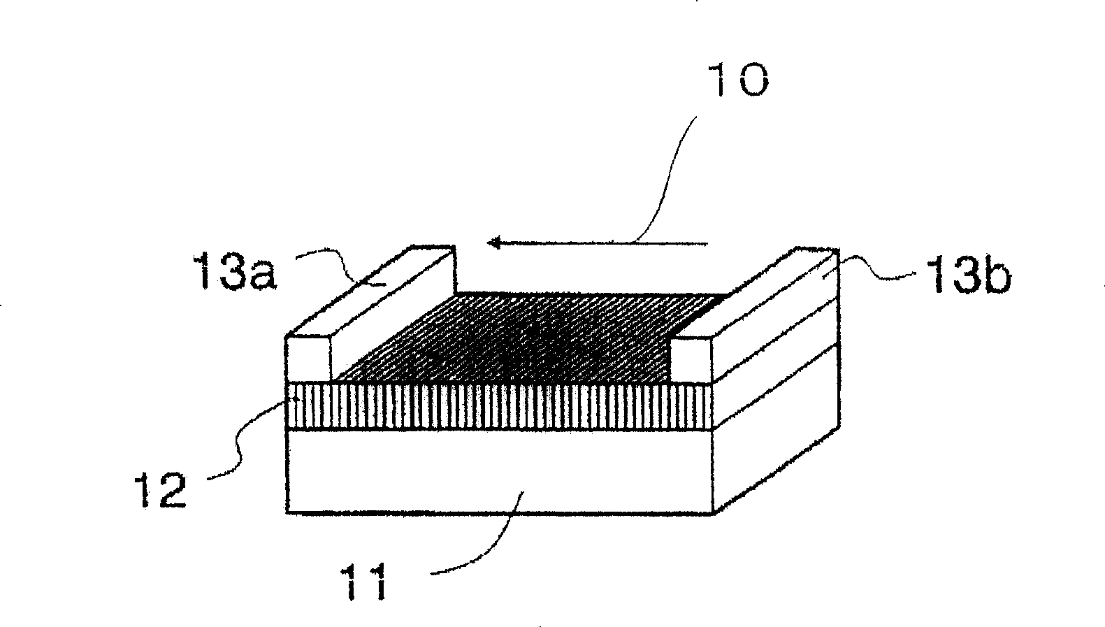
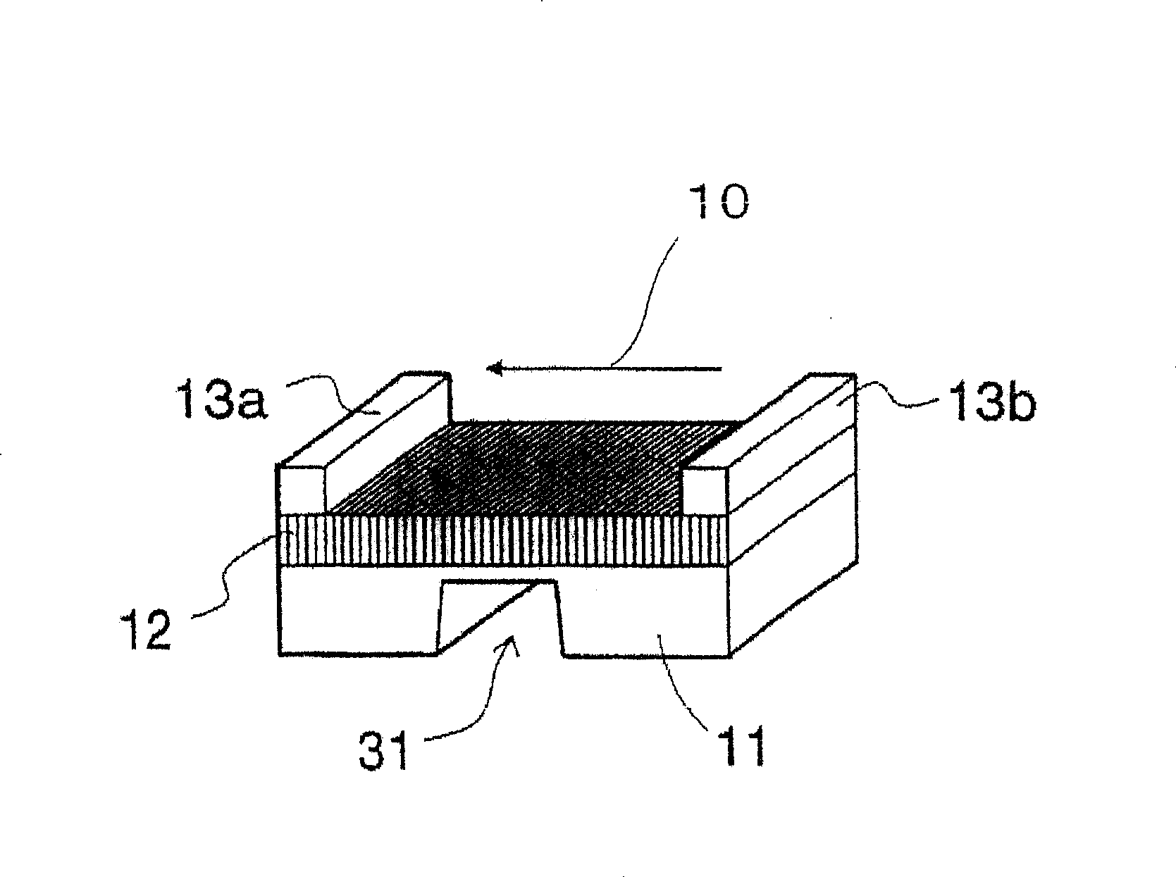
[0053] figure 1 The shown thermoelectric conversion device has: a plate-shaped base 11 ; a thermoelectric conversion film 12 on the base 11 ;
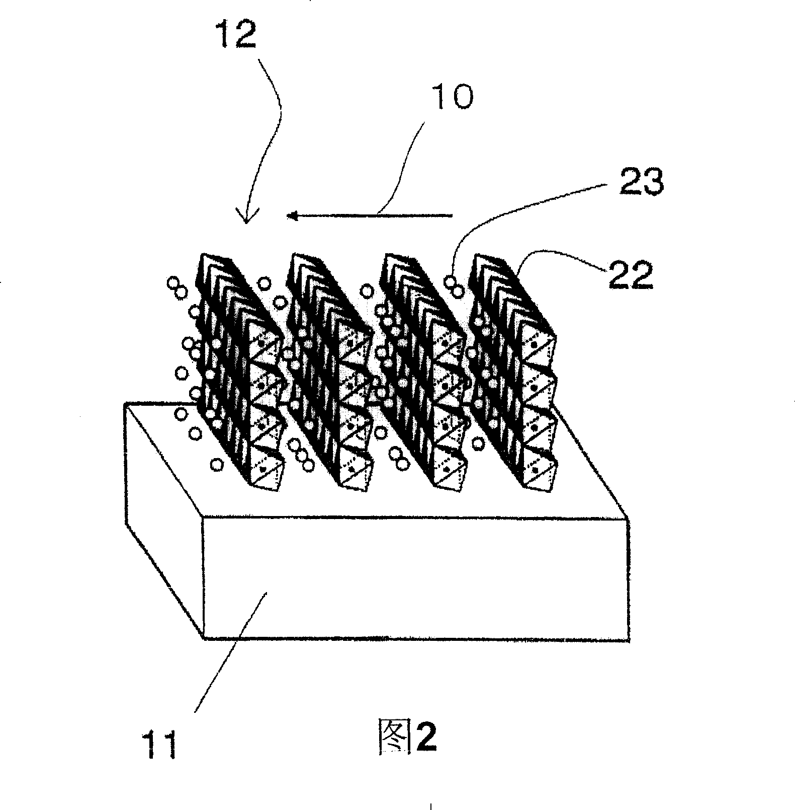
[0054] FIG. 2 illustrates the crystal structure of the thermoelectric conversion film 12 . The thermoelectric conversion film 12 has a layered structure in which electrically conductive layers 22 and electrically insulating layers 23 are alternately arranged. That is, the thermoelectric conversion film 12 is composed of a crystalline thin film in which electrically conductive layers 22 and electrically insulating layers 23 are alternately arranged.
[0055] In crystallography, the interlayer direction, that is, the direction perpendicular to the layer is called the c-axis direction 10 . A pair of electrodes 13 a , 13 b is arranged so that current can flow in the c-axis direction 10 .
[0056] The thermoelectric conversion film 12 is an epitaxial thin film (epitaxially grown film), and the c-axis direction 10 has orientation along th...
Embodiment 1
[0099] Sapphire Al of 10mm square and 100μm thick 2 o 3 On the A-side substrate, the layered oxide Na 0.4 CoO 2 film formation. The film formation method is to use a 4-inch diameter Na 0.5 CoO 2 RF magnetron sputtering of sintered targets.
[0100] 80% Ar, 20% O 2 The atmosphere was maintained at 5.0Pa, and after pre-sputtering was performed for 1 hour at an output power of 60W, deposition was performed on a substrate heated to 700°C for 5 hours under the same conditions as during pre-sputtering, and thereafter, the The thin film on the heated substrate was cooled to room temperature in an oxygen atmosphere for 2 hours, and as a result, a thin film having a film thickness of 1000 nm and having a metallic luster was obtained.
[0101] The composition ratio of Na and Co in the thin film was confirmed to be about Na:Co=0.4:1 by energy dispersive fluorescent X-ray analysis.
[0102] Na 0.4 CoO 2 The results of X-ray diffraction measurement of the film are shown in Figu...
Embodiment 2
[0117] used by CaO 2 、Co 3 o 4 A 4-inch raw material target (target) composed of a powder sintered body was grown on a 10 mm square, 100 μm thick sapphire M-plane substrate with a film thickness of 1000 nm under the same sputtering conditions as in Example 1.
[0118] It was confirmed by energy dispersive fluorescent X-ray analysis that the composition ratio of Ca and Co in this thin film was approximately Ca:Co=0.5:1. the Ca 0.5 CoO 2 The results of X-ray diffraction measurement of the film are shown in Figure 9 . In addition to the diffraction peak due to the sapphire substrate, only an index sub-peak based on (020) due to the diffraction of the thin film was observed.
[0119] It was thus confirmed that Ca 0.5 CoO 2 The film is epitaxially grown with the (010) plane parallel to the substrate. In addition, it was confirmed by 4-axis X-ray diffraction measurement that Ca 0.5 CoO 2 The c-axis of the crystals is oriented in-plane of the film.
[0120] Ca 0.5 CoO ...
PUM
 Abstract
Description
Claims
Application Information


