Compound semiconductors and their application

a technology of compound semiconductors and semiconductors, applied in the direction of nickel compounds, non-metal conductors, conductors, etc., can solve the problems that many conventional compound semiconductors fail to meet all of these conditions at once, and achieve good thermoelectric conversion performance and improve zt value

Active Publication Date: 2013-12-10
LG CHEM LTD
View PDF12 Cites 2 Cited by
  • Summary
  • Abstract
  • Description
  • Claims
  • Application Information

AI Technical Summary

Benefits of technology

[0024]According to the present disclosure, a new compound semiconductor material is provided.
[0025]In one aspect, the new compound semiconductor may replace a conventional compound semiconductor or may be used as another material in addition to the conventional compound semiconductor.
[0026]Further, in one aspect of the present disclosure, since the compound semiconductor has good thermoelectric conversion performance, it may be used for a thermoelectric conversion device. In particular, the compound semiconductor according to the present disclosure may have an improved ZT value, which is a thermoelectric performance index, since the thermal conductivity is improved. Therefore, the compound semiconductor according to the present disclosure may be used as a thermoelectric conversion material of a thermoelectric conversion device.
[0027]In addition, in another aspect of the present disclosure, the compound semiconductor may be used for a solar cell. Particularly, the compound semiconductor of the present disclosure may be used as a light absorption layer of the solar cell.
[0028]Moreover, in another aspect of the present disclosure, the compound semiconductor may be used for an IR window or IR sensor which selectively passes IR, a magnetic device, a memory or the like.

Problems solved by technology

However, many conventional compound semiconductors fail to meet all of these conditions at once.

Method used


Image

  • Compound semiconductors and their application
  • Compound semiconductors and their application

Examples


examples

[0060]Hereinafter, embodiments of the present disclosure will be described in detail. The embodiments of the present disclosure, however, may take several other forms, and the scope of the present disclosure should not be construed as being limited to the following examples. The embodiments of the present disclosure are provided to more fully explain the present disclosure to those having ordinary knowledge in the art to which the present disclosure pertains.

example

[0061]0.0497 g of In, 0.0113 g of Zn, 0.3522 g of Co, 0.0713 g of Rh, 2.2149 g of Sb, 0.1028 g of Sn, 0.1768 g of Te and 0.0209 g of Co3O4 were prepared as reagents, and were mixed by using mortar. The materials mixed as above were put into a silica tube and vacuum-sealed and then heated at 650° C. for 36 hours. The time for raising the temperature to 650° C. was 1 hour and 30 minutes, and In0.25Zn0.1Co3.6Rh0.4Sb10.5Sn0.5O0.2Te0.8 powder was obtained.

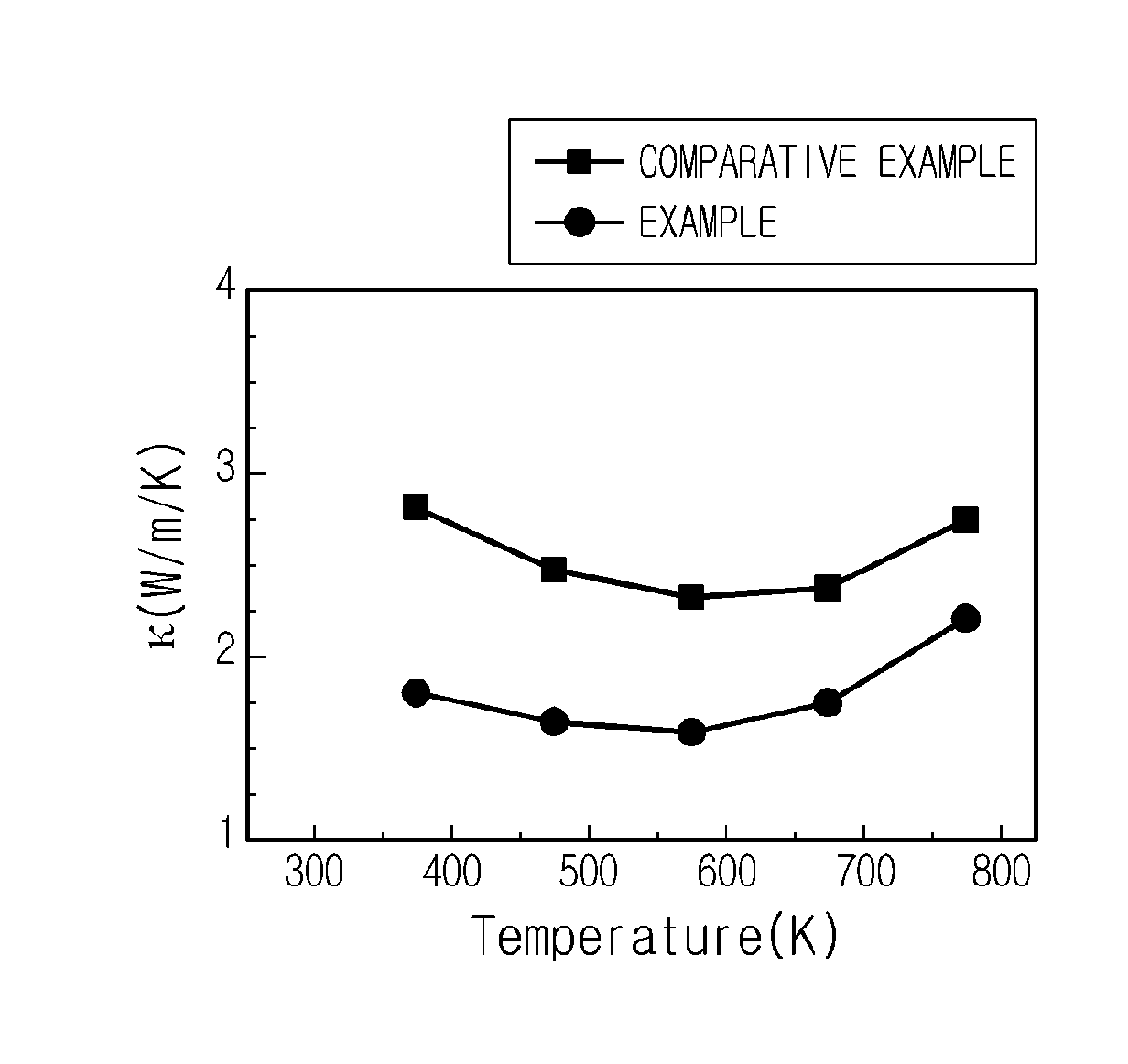
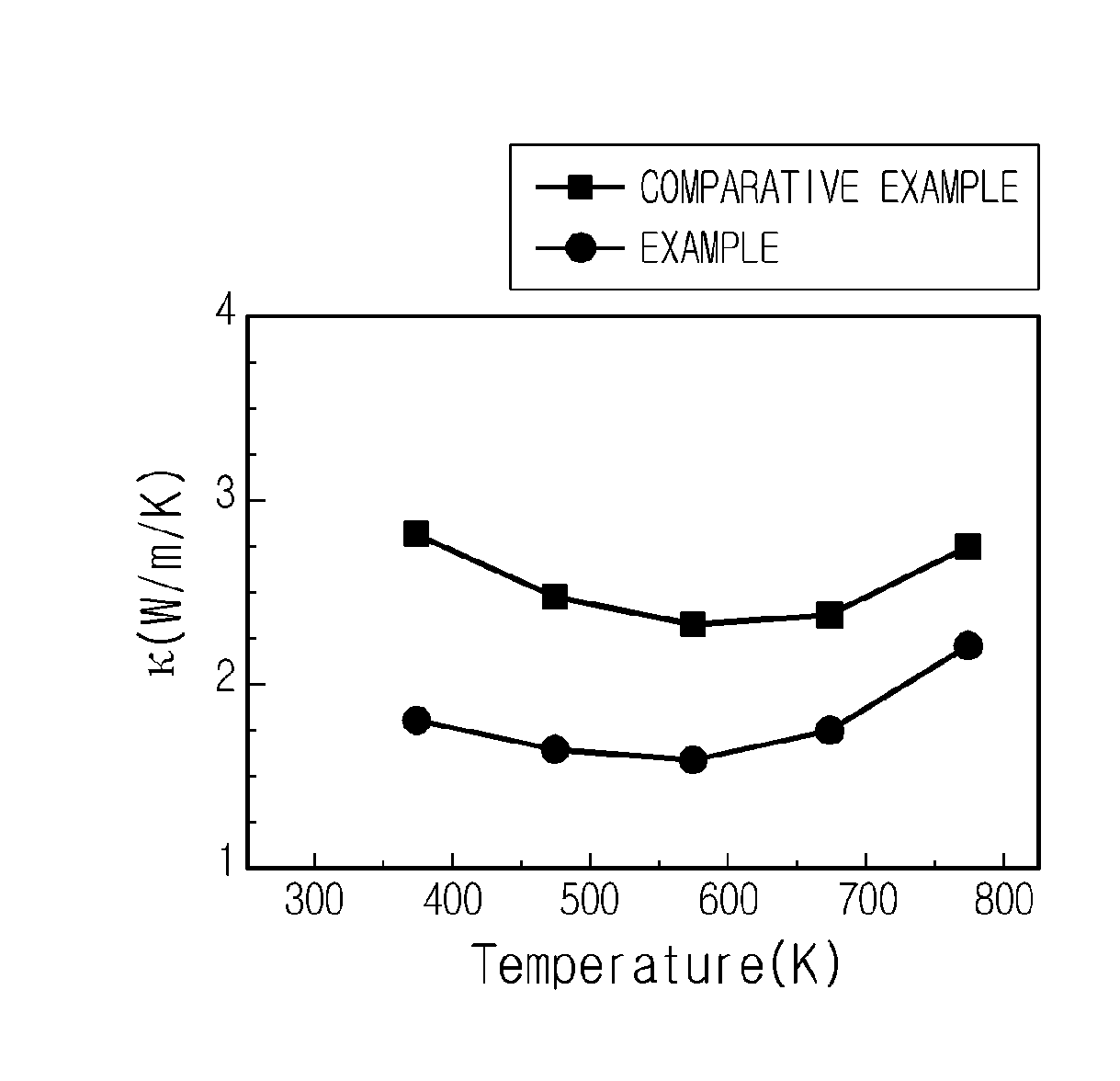
[0062]A part of the composed materials prepared above was formed into a disk having a diameter of 10 mm and a thickness of 1 mm. After that, a pressure of 200 MPa was applied thereto by using a CIP (Cold Isostatic Pressing). Subsequently, the obtained result was put into a quartz tube and vacuum-sintered for 12 hours. In regard to the sintered disk, thermal conductivity was measured by using LFA457 (Netzsch, Inc) at predetermined temperature intervals. The measurement result is shown in FIG. 1 as Example.


PUM

PropertyMeasurementUnit
temperatureaaaaaaaaaa

Abstract

Disclosed are new compound semiconductors which may be used for solar cells or as thermoelectric materials, and their application. The compound semiconductor may be represented by a chemical formula: InxMyCo4-mAmSb12-n-z-pXnQ′pTez, where M is at least one selected from the group consisting of Ca, Sr, Ba, Ti, V, Cr, Mn, Cu, Zn, Ag, Cd, Sc, Y, La, Ce, Pr, Nd, Sm, Eu, Gd, Tb, Dy, Ho, Er, Tm, Yb and Lu; A is at least one selected from the group consisting of Fe, Ni, Ru, Rh, Pd, Ir and Pt; X is at least one selected from the group consisting of Si, Ga, Ge and Sn; Q′ is at least one selected from the group consisting of O, S and Se; 0<x<1; 0<y<1; 0≦m≦1; 0≦n≦7; 0<z≦2 and 0<p≦2.

Description

CROSS-REFERENCE TO RELATED APPLICATION[0001]This application is a continuation of International Application No. PCT / KR2012 / 003733 filed on May 11, 2012, which claims priority to Korean Patent Application No. 10-2011-0045348 filed on May 13, 2011, Korean Patent Application No. 10-2011-0045349 filed on May 13, 2011, Korean Patent Application No. 10-2011-0049609 filed on May 25, 2011 and Korean Patent Application No. 10-2012-0050261 filed on May 11, 2012 in the Republic of Korea, the entire contents of which are incorporated herein by reference.TECHNICAL FIELD[0002]The present disclosure relates to a new compound semiconductor material which may be used for solar cells or as thermoelectric materials, its preparation method, and its applications.BACKGROUND ART[0003]A compound semiconductor is not a single element such as silicon and germanium but a compound having two or more kinds of combined elements serving as a semiconductor. Various kinds of compound semiconductors have been develo...

Claims


Application Information

Patent Timeline
Patent Type & Authority Patents(United States)
IPC IPC(8): H01B1/02
CPCC01G51/006C01G53/006C01G55/002C01B19/002H01L35/18H01L31/032C01P2006/32C01P2006/40C01P2002/50C01P2002/88C01P2004/20H10N10/853C01B19/00C01G15/00C01G51/00C01G30/00
Inventor PARK, CHEOL-HEEKIM, TAE-HOON
Owner LG CHEM LTD
Why Eureka
Try Eureka