Fabricating method of semiconductor package structure

a technology of semiconductor packaging and fabrication method, which is applied in the direction of semiconductor devices, semiconductor/solid-state device details, electrical devices, etc., can solve the problems of reducing the strength of the adhesive layer, poor heat conduction, and providing a higher bonding, and achieves low cte properties and better heat dissipation efficiency.

Active Publication Date: 2013-01-10
SUBTRON TECH
View PDF4 Cites 0 Cited by
  • Summary
  • Abstract
  • Description
  • Claims
  • Application Information

AI Technical Summary

Benefits of technology

[0007]Accordingly, the invention is directed to a semiconductor package structure having better heat dissipation efficiency and low CTE property.
[0029]Based on the depiction above, since the semiconductor die of the invention is disposed in the containing cavity located on an end of the heat conductive post, so that the heat produced by the semiconductor die can be fast transferred to outside directly through the heat conductive post and the carrier under the semiconductor die. As a result, the semiconductor package structure of the invention has a better heat dissipation efficiency.

Problems solved by technology

Along with gradually increasing the bonding point density of a chip, the leadframe is unable to provide a higher bonding point density, so that it is replaced by a package substrate with high bonding point density, where the chip is packed onto the package substrate through conductive media such as metal wires or bumps.
When paste, for example a silver epoxy, is used as the material of the adhesive layer, due to the poor thermal conducting rate (less than 20 W / mK), high coefficient of thermal expansion (CTE) (greater than 30 ppm / K) and poor adhering strength of the silver epoxy, so that when the heat produced by the chip is transferred to the package substrate through the adhesive layer, an increasing thermal resistance is caused by the adhesive layer, which further leads to poor heat conduction and decrease the strength of the adhesive layer and even destroy the adhesive layer when thermal stress occurs.

Method used


Image

  • Fabricating method of semiconductor package structure
  • Fabricating method of semiconductor package structure
  • Fabricating method of semiconductor package structure

Examples


Embodiment Construction

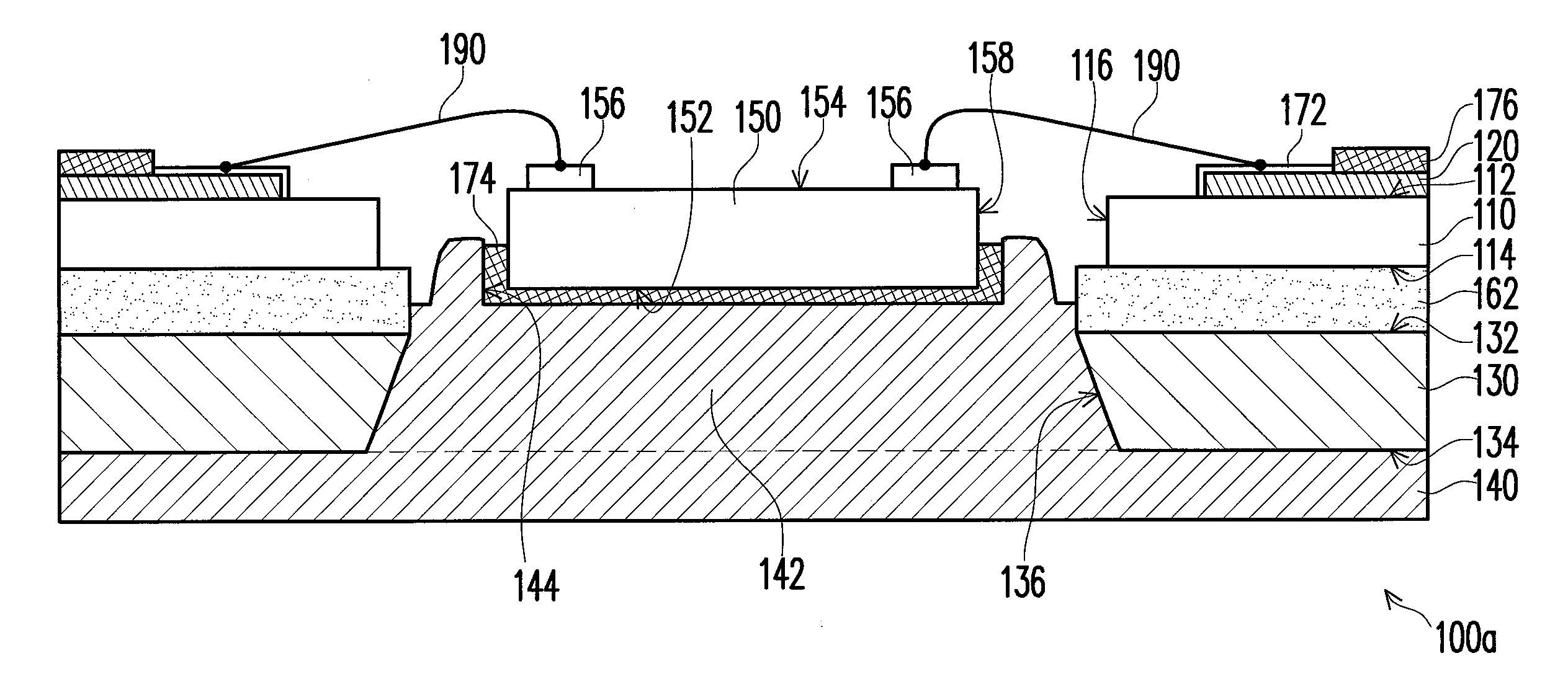
[0035]FIG. 1 is a cross-sectional diagram of a semiconductor package structure according to an embodiment of the invention. Referring to FIG. 1, in the embodiment, a semiconductor package structure 100a includes a dielectric layer 110, a patterned metal layer 120, a carrier 130, a metal layer 140 and a semiconductor die 150.

[0036]In more details, the dielectric layer 110 has a first surface 112 and a second surface 114 opposite to the first surface 112 and an opening 116, in which the opening 116 goes through the first surface 112 and the second surface 114. The patterned metal layer 120 is disposed on the first surface 112 of the dielectric layer 110, in which the patterned metal layer 120 exposes the first surface 112 of a portion of the metal layer 110. In the embodiment, the patterned metal layer 120 can serve as the bonding pad for a successive wire bonding process. The carrier 130 is disposed at the second surface 114 of the dielectric layer 110 and has a third surface 132 and...


PUM

PropertyMeasurementUnit
heat conductiveaaaaaaaaaa
stressaaaaaaaaaa
heat conductivityaaaaaaaaaa

Abstract

A fabricating method of a semiconductor package structure is provided. A dielectric layer having a first surface and a second surface is provided. A patterned metal layer has been formed on the first surface of the dielectric layer. An opening going through the first and the second surfaces is formed. A carrier having a third surface and a fourth surface is formed at the second surface. A portion of the third surface is exposed by the opening of the dielectric layer. A semiconductor die having a joining surface and a side-surface is joined in the opening. At least a through hole going through the third and the fourth surfaces is formed. A metal layer having at least a heat conductive post extending from the fourth surface of the carrier to the through hole and disposed in the through hole and a containing cavity is formed on the fourth surface.

Description

CROSS-REFERENCE TO RELATED APPLICATION[0001]This application is a divisional of and claims the priority benefit of U.S. application Ser. No. 12 / 915,514, filed on Oct. 28, 2010, now pending, which claims the priority benefit of Taiwan application serial no. 99122521, filed on Jul. 8, 2010. The entirety of the above-mentioned patent applications is hereby incorporated by reference herein and made a part of specification.BACKGROUND OF THE INVENTION[0002]1. Field of the Invention[0003]The invention generally relates to a package structure and a fabricating method thereof, and more particularly, to a package and the carrier structure thereof and a fabricating method thereof with demand on high heat conduction performing.[0004]2. Description of Related Art[0005]The purpose of chip package is to provide a chip with an appropriate signal path, a heat conduction path and structure protection. The traditional wire bonding technique usually adopts a leadframe as a carrier of the chip. Along wi...

Claims


Application Information

Patent Timeline
Patent Type & Authority Applications(United States)
IPC IPC(8): H01L21/50
CPCH01L23/13H01L24/32H01L23/3731H01L23/3732H01L23/498H01L23/562H01L2224/73265H01L2224/32225H01L2224/32245H01L2224/48227H01L2924/01019H01L23/3677H01L24/83H01L2224/83001H01L2224/32257H01L2224/92247H01L2924/00012H01L2924/00H01L2924/351H01L2924/12042H01L24/73H01L2924/15153
Inventor TSENG, TZYY-JANGWANG, CHIN-SHENGCHUANG, CHIH-HONG
Owner SUBTRON TECH
Why Eureka
Try Eureka