Device contactor with integrated RF shield

a contactor and device technology, applied in the direction of measurement devices, instruments, instrument screening arrangements, etc., can solve the problems of rf shield directly coupled to a pcb not fully sealing all possible entry points, permanent coating of conductive/dissipative materials over a device, and inability to reuse for testing other devices and their associated circuitry

Inactive Publication Date: 2013-01-17
TEXAS INSTR INC
View PDF62 Cites 19 Cited by
  • Summary
  • Abstract
  • Description
  • Claims
  • Application Information

AI Technical Summary

Benefits of technology

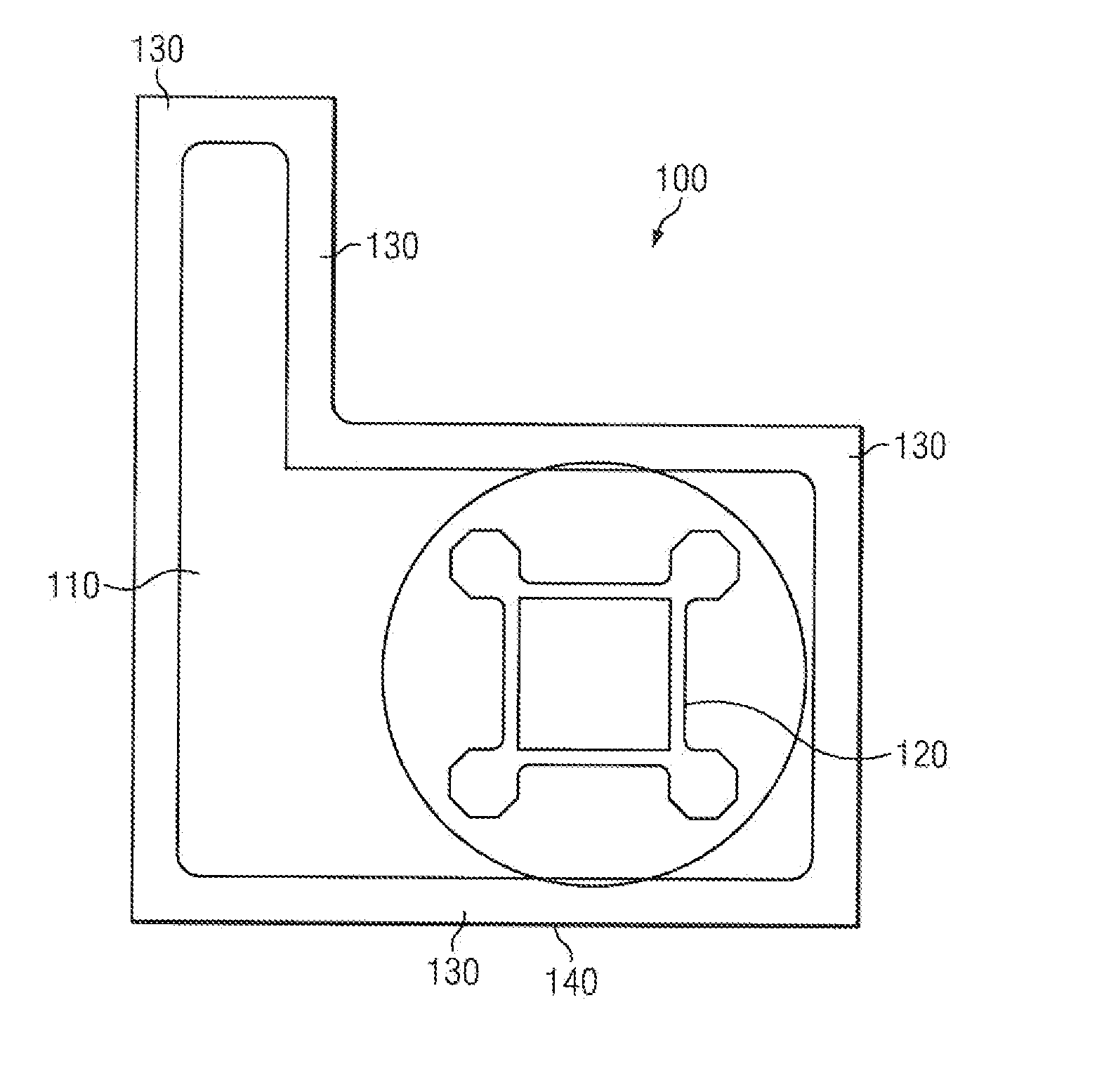
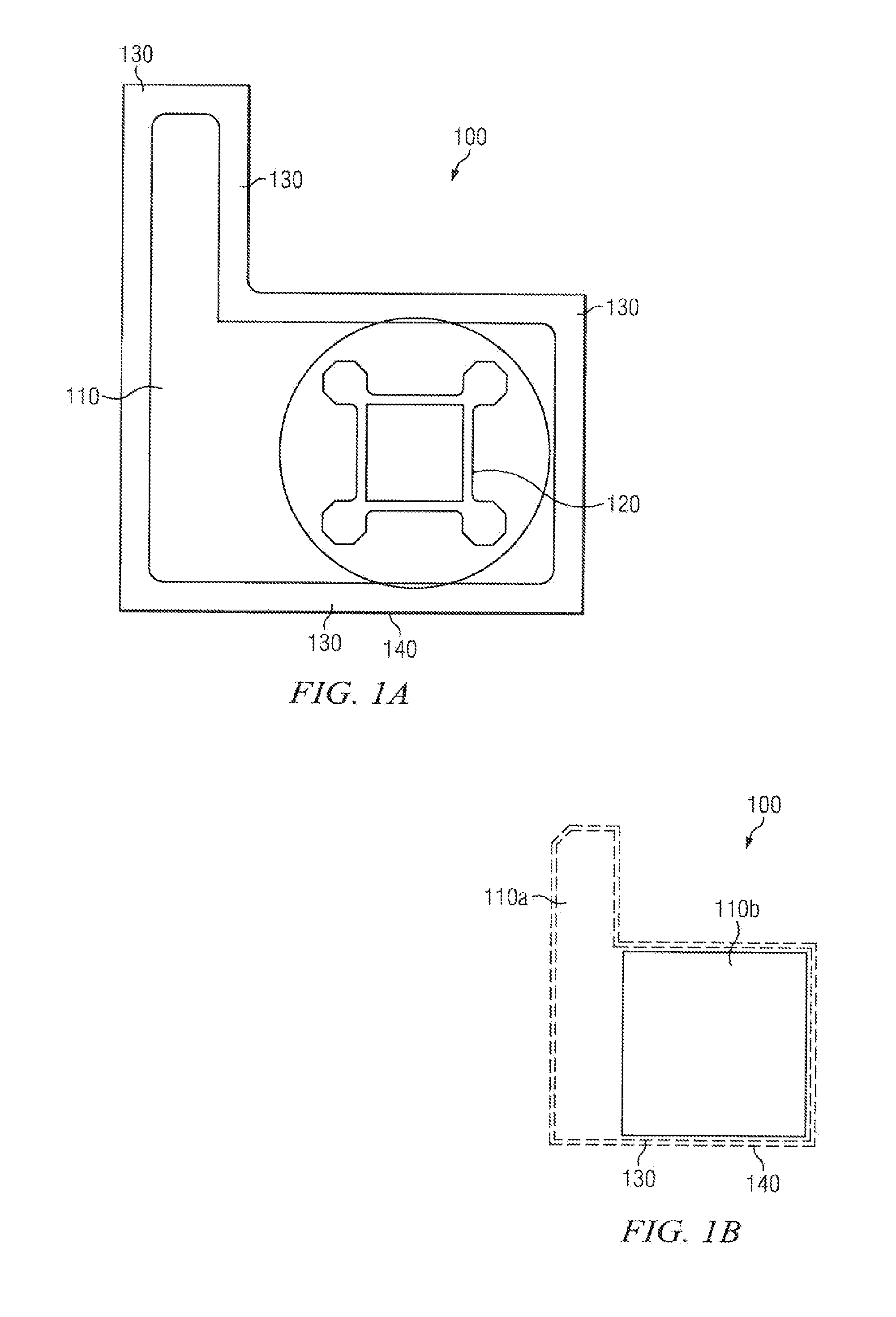
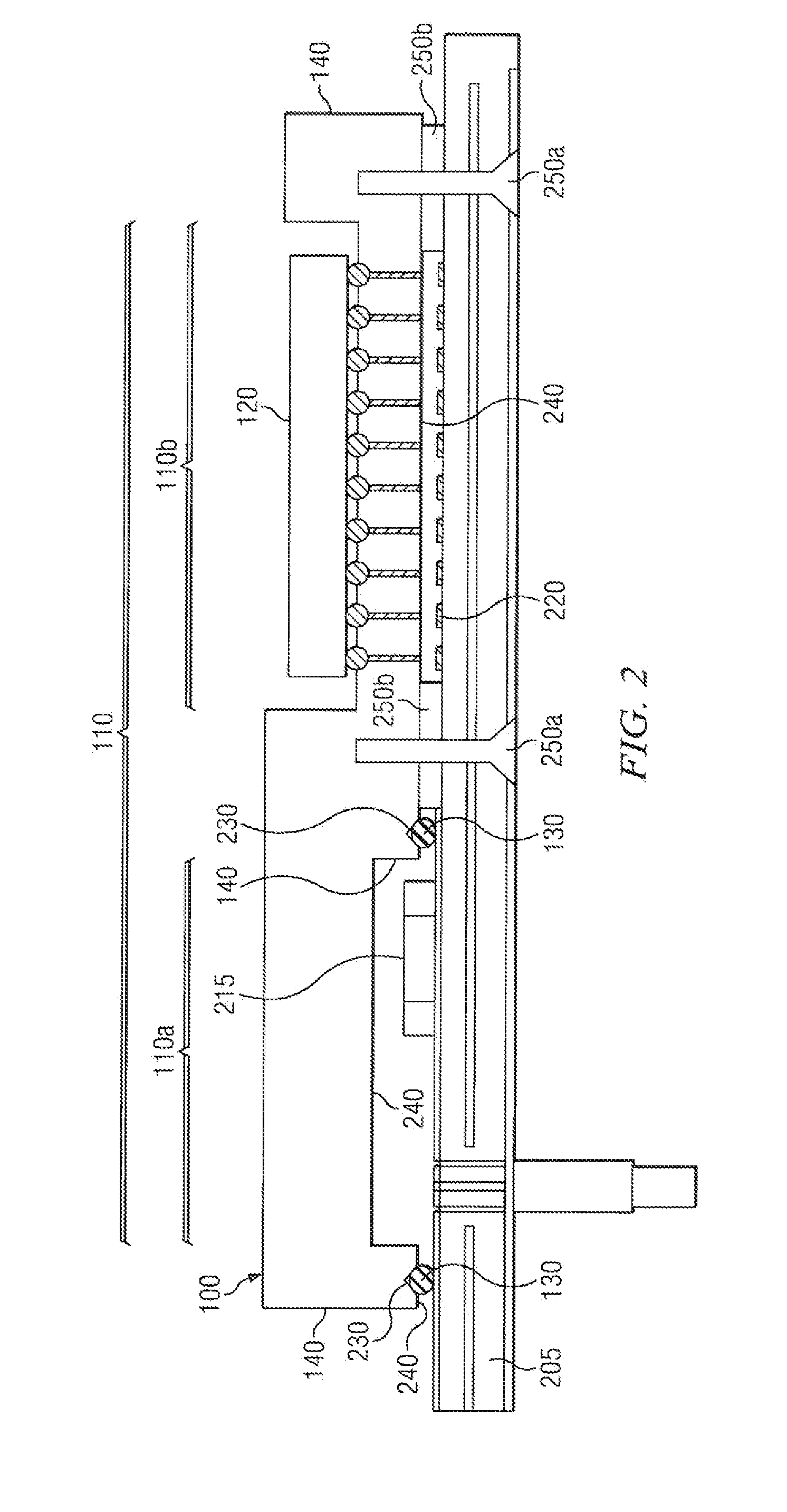
[0005]Applicants have recognized that there is a need for methods and apparatus for shielding a device under test and nearby circuitry on a printed circuit board (“PCB”), such as a load board, from RF and EM interference. Applicants have also recognized that an RF shield directly coupled to a PCB does not fully seal all possible entry points for external radiation. Applicants have further recognized that a permanent coating of conductive / dissipative material over a device, in addition to shielding only the device and not the nearby circuitry, cannot be reused for testing other devices and their associated circuitry. Therefore, it is a technical advantage to provide an RF shield operationally attached to a device contactor instead of a device, such that when the device contactor is docked or removably attached to a PCB, the RF shield forms a Faraday cage. It is a further technical advantage to incorporate a conductive shield gasket operationally attached to the device contactor, to seal all possible entry points for external radiation when the device contactor is docked or attached to a PCB.

Problems solved by technology

Applicants have also recognized that an RF shield directly coupled to a PCB does not fully seal all possible entry points for external radiation.
Applicants have further recognized that a permanent coating of conductive / dissipative material over a device, in addition to shielding only the device and not the nearby circuitry, cannot be reused for testing other devices and their associated circuitry.
While the copper foil reduced RF and EM noise penetration, the foil did not facilitate an easy removal and a complete seal, and thus left some gaps through which RF and EM noise could still affect the devices under test.
Moreover, the copper foil was too thin to fully shield the devices under test, even within space covered by the copper foil.

Method used


Image

  • Device contactor with integrated RF shield
  • Device contactor with integrated RF shield
  • Device contactor with integrated RF shield

Examples


Embodiment Construction

[0018]Reference will now be made in detail to the exemplary embodiments, an example of which is illustrated in the accompanying drawings. Wherever possible, the same reference numbers will be used throughout the drawings to refer to the same or like parts.

[0019]In the following description, reference is made to the accompanying drawings that form a part thereof, and in which is shown by way of illustration specific exemplary embodiments in which may be practiced. These embodiments are described in sufficient detail to enable those skilled in the art to practice these embodiments and it is to be understood that other embodiments may be utilized and that changes may be made without departing from the scope of the invention. The following description is, therefore, merely exemplary.

[0020]Notwithstanding that the numerical ranges and parameters setting forth the broad scope of the exemplary embodiments are approximations, the numerical values set forth in the specific examples are repor...


PUM


Abstract

An apparatus includes a device contactor having an integrated radio frequency (“RF”) shield and a gasket coupled to a first surface of the device contactor. When the device contactor is removably attached to a printed circuit board (“PCB”), the gasket contacts the PCB, and the RF shield and the gasket form a Faraday cage that shields a device under test and/or circuitry associated with the device under test from RF noise.

Description

FIELD OF THE INVENTION[0001]This invention relates generally to the field of semiconductor devices and device testing, and more particularly, to methods and apparatus for shielding a device under test and nearby circuitry from noise and interference.DESCRIPTION OF THE RELATED ART[0002]In testing or measuring electrical properties of integrated circuit (“IC”) devices in a post-production stage, each IC device is connected to an IC tester through a load board electrically connected to respective electrodes of the IC device. For this purpose, one or more device contactors are typically mounted on the load board and serve as part of a contacting mechanism for IC devices under test. During a test, IC devices are coupled to the device contactors to electrically connect the IC devices to the IC tester.[0003]Existing device contactor designs do not completely shield a device under test and nearby circuitry on a load board from radio frequency (“RF”) and electromagnetic (“EM”) interference, ...

Claims


Application Information

Patent Timeline
Patent Type & Authority Applications(United States)
IPC IPC(8): H05K9/00
CPCH05K9/0024G01R1/18G01R1/0466
Inventor KORSON, MICHAEL PATRICKGUIDRY, DAVID WALKER
Owner TEXAS INSTR INC
Why Eureka
Try Eureka