
Group iii nitride semiconductor light-emitting device

a technology of nitride and semiconductor, applied in the direction of semiconductor devices, basic electric elements, electrical appliances, etc., can solve the problems of reducing light emission performance, reducing contact resistance, and remarkably increasing consumption, so as to reduce contact resistance and reduce consumption

Active Publication Date: 2013-01-24
TOYODA GOSEI CO LTD
View PDF8 Cites 4 Cited by
  • Summary
  • Abstract
  • Description
  • Claims
  • Application Information

AI Technical Summary

Benefits of technology

The present invention provides a Group III nitride semiconductor light-emitting device with reduced contact resistance between the p contact layer and the transparent electrode. This is achieved by using a p-type doped material, such as Mg, which forms bonds with oxygen on the interface between the p contact layer and the transparent electrode, thereby reducing the contact resistance. The material of the structure can be undoped or p-type doped, with the preferred composition ratio being 15-30 mol%. The structure also has a height of 0.5-5 nm to further reduce the contact resistance. The present invention can improve the performance and reliability of the light-emitting device.

Problems solved by technology

Therefore, the power consumption is remarkably increased due to resistance, causing reduction in light emission performance.
Such a structure can reduce the contact resistance.
However, even with the method disclosed by Japanese Patent Application Laid-Open (kokai) No. 2006-80469 or 2005-260245, the contact resistance between the p contact layer and the ITO electrode is not sufficiently reduced, and further reduction technique is desired.

Method used


Image

  • Group iii nitride semiconductor light-emitting device
  • Group iii nitride semiconductor light-emitting device
  • Group iii nitride semiconductor light-emitting device

Examples


embodiment 1

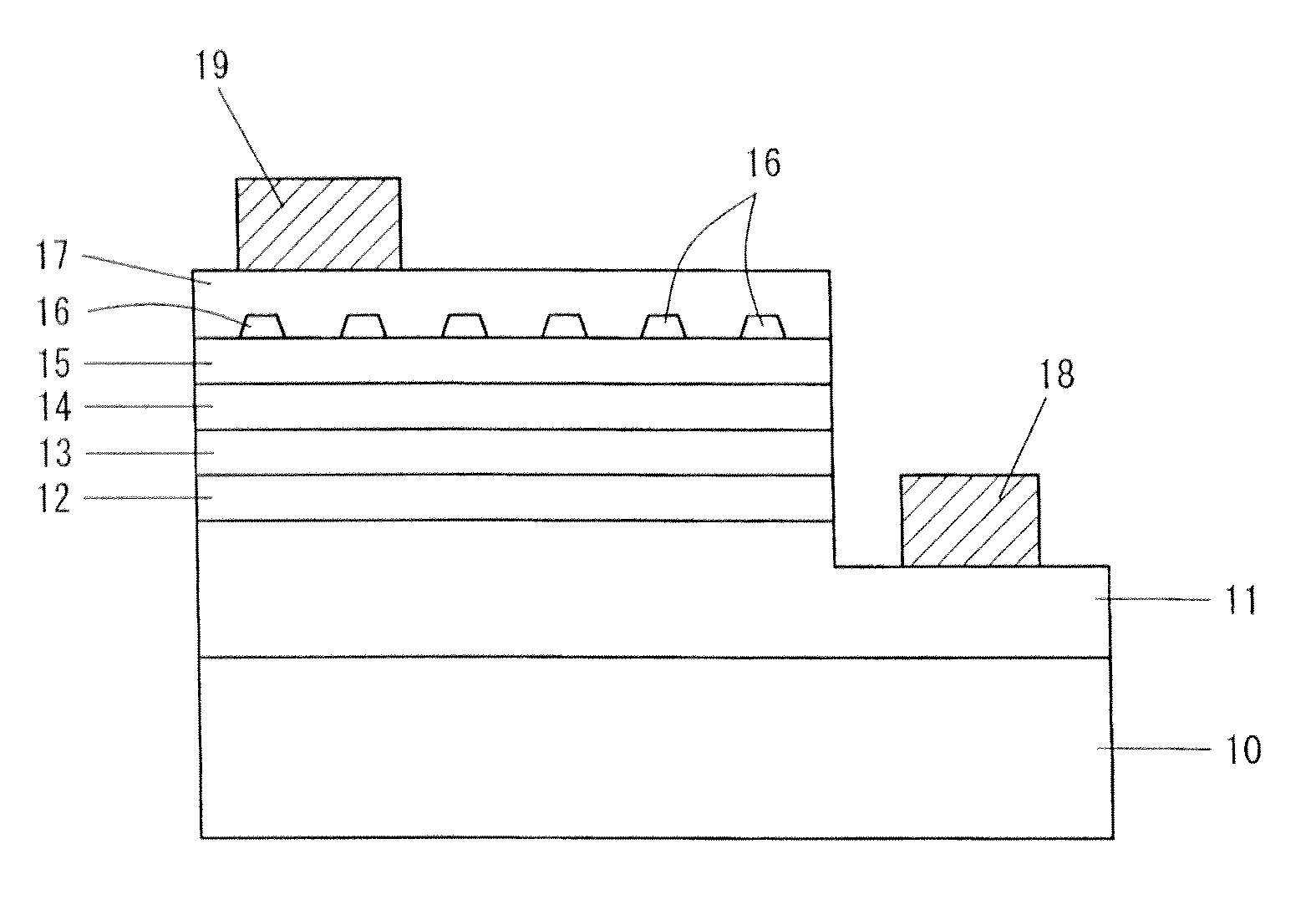
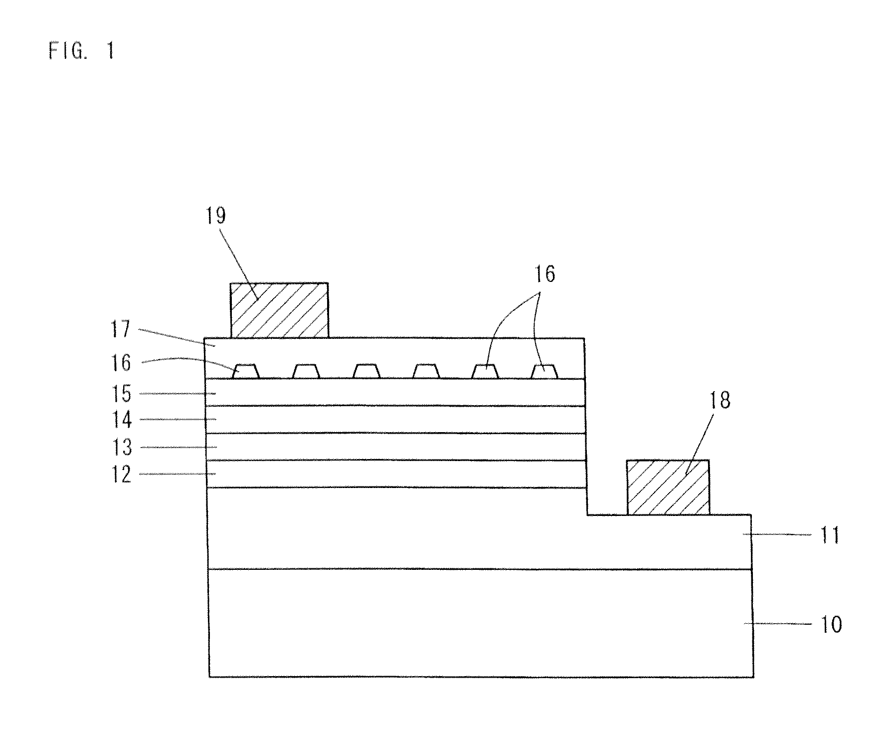
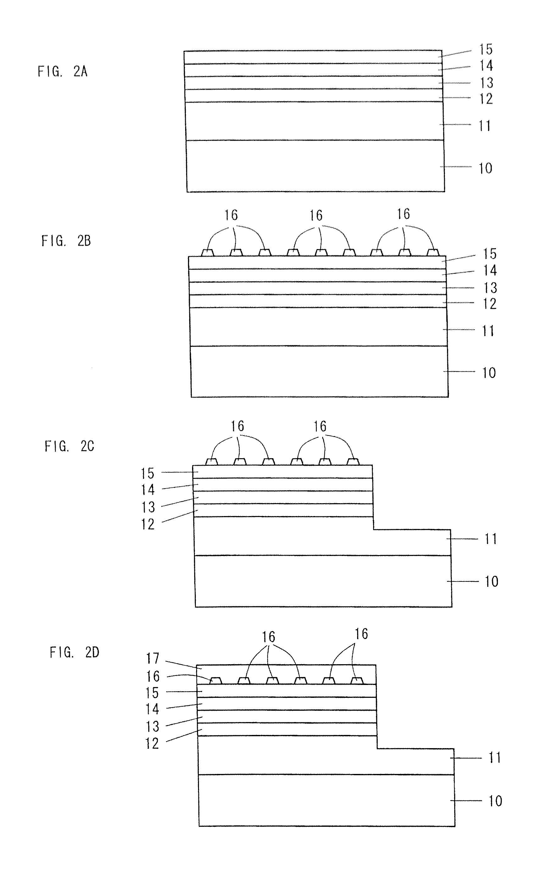
[0030]FIG. 1 shows the configuration of a Group III nitride semiconductor light-emitting device according to Embodiment 1. The Group III nitride semiconductor light-emitting device according to Embodiment 1 includes a sapphire substrate 10; an n contact layer 11, an n cladding layer 12, a light-emitting layer 13, a p cladding layer 14, and a p contact layer 15, which are sequentially deposited on the sapphire substrate 10. Moreover, a trench having a depth extending from the top surface of the p-type contact layer 15 to the n contact layer 11 is formed, and an n electrode 18 is formed on the n-type contact layer 11 exposed at the bottom of the trench. A dot-like structure 16 is formed on the p contact layer 15, in which a plurality of AlGaN dots are discretely distributed. An ITO electrode 17 is formed on the p contact layer 15 and the dot-like structure 16. A p electrode 19 is formed on the ITO electrode 17.

[0031]On the surface of the sapphire substrate 10, which surface is at the ...


PUM

PropertyMeasurementUnit
thicknessaaaaaaaaaa
thicknessaaaaaaaaaa
thicknessaaaaaaaaaa

Abstract

A Group III nitride semiconductor light-emitting device exhibiting reduced contact resistance between a p contact layer and an ITO electrode. The Group III nitride semiconductor light-emitting device has an AlGaN dot-like structure on the p contact layer, and an ITO electrode on the p contact layer and the dot-like structure. The dot-like structure has a structure in which a plurality of AlGaN dots are discretely distributed on the top surface of the p contact layer. The dot-like structure is bonded to oxygen, and oxygen increases on an interface between the p contact layer and the ITO electrode.

Description

BACKGROUND OF THE INVENTION[0001]1. Field of the Invention[0002]The present invention relates to a Group III nitride semiconductor light-emitting device exhibiting reduced contact resistance between a p contact layer and an ITO electrode.[0003]2. Background Art[0004]In recent years, there has been an expanding demand for general illumination applications of Group III nitride semiconductor light-emitting devices, and high-power light-emitting devices are being developed. Every year, the driving current is increasing with the development of high-power light-emitting devices. Therefore, the power consumption is remarkably increased due to resistance, causing reduction in light emission performance. To avoid this, the resistance of light-emitting devices must be reduced.[0005]Most of Group III nitride semiconductor light-emitting devices currently produced are of a lateral conductive face-up type or flip-chip type. In the face-up type device, an ITO transparent electrode is formed on al...

Claims


Application Information

Patent Timeline
Patent Type & Authority Applications(United States)
IPC IPC(8): H01L33/42
CPCH01L33/38H01L33/42H01L33/40
Inventor MAKINO, HIROAKISAITO, YOSHIKI
Owner TOYODA GOSEI CO LTD
Learn More