Current-limiting layer and a current-reducing layer in a memory device

a memory device and current-limiting layer technology, applied in the field of resistance switching memory devices, can solve the problems of undesirable alteration or disturbance of the “logic” state of the interconnected memory cells/devices, the current flowing through the current carrying lines in the memory array, and the scaling issue of traditional nonvolatile memory technology, etc., to minimize the overall power consumption of the memory array and reduce the level of current flowing

Active Publication Date: 2013-01-31
SANDISK TECH LLC +1
View PDF9 Cites 83 Cited by
  • Summary
  • Abstract
  • Description
  • Claims
  • Application Information

AI Technical Summary

Benefits of technology

[0011]Embodiments of the invention generally include a method of forming a ReRAM type nonvolatile memory device. The ReRAM type switching memory device includes at least one current-limiting layer and at least one current-reducing layer integrated within or adjacent to a ReRAM type nonvolatile memory element. The ReRAM type switching memory element may include a first electrode layer, a second e

Problems solved by technology

However, as device dimensions shrink, scaling issues pose challenges for traditional nonvolatile memory technology.
A large current flowing through the current carrying lines in a memory array can also undesirably alte

Method used


Image

  • Current-limiting layer and a current-reducing layer in a memory device
  • Current-limiting layer and a current-reducing layer in a memory device
  • Current-limiting layer and a current-reducing layer in a memory device

Examples


examples

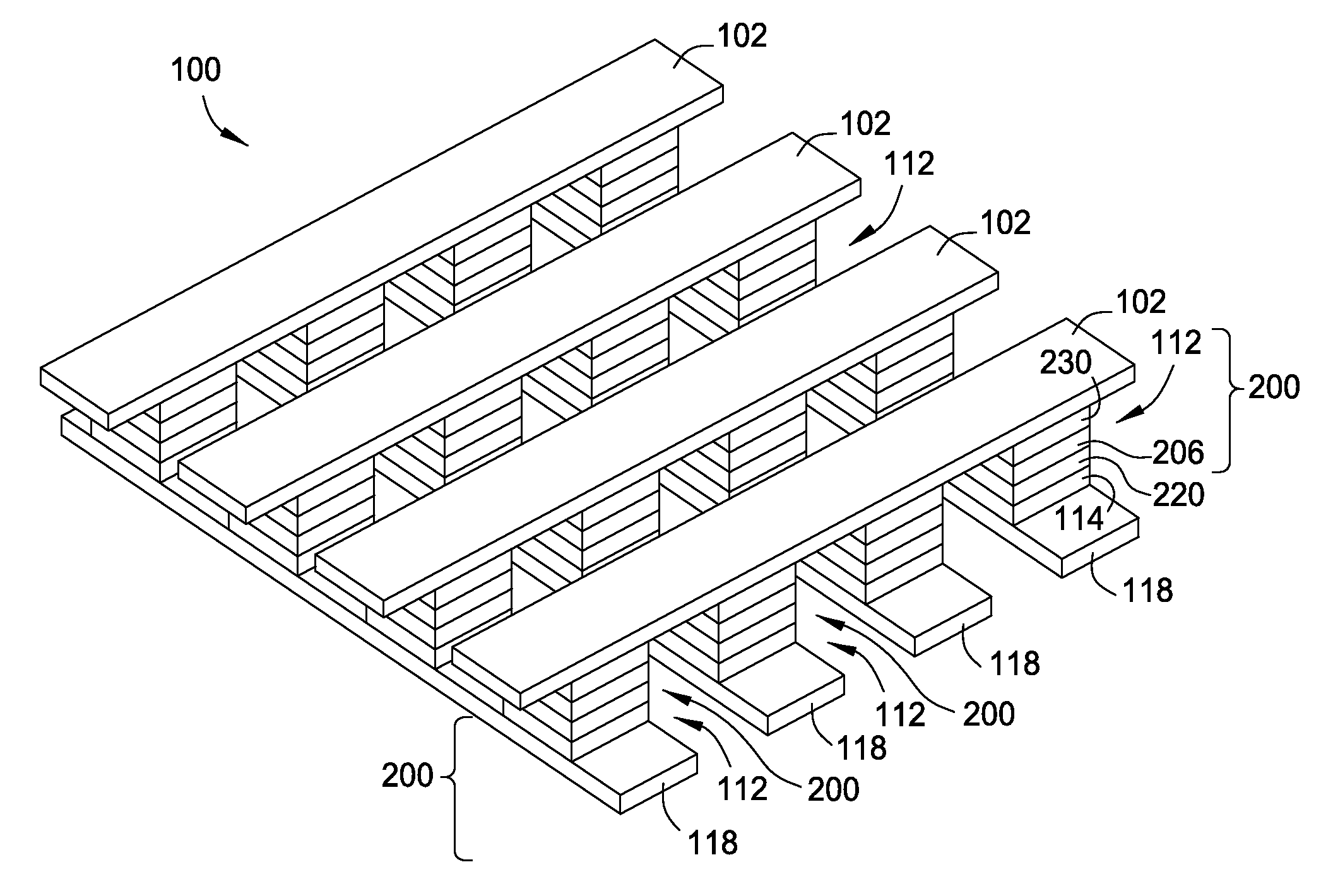
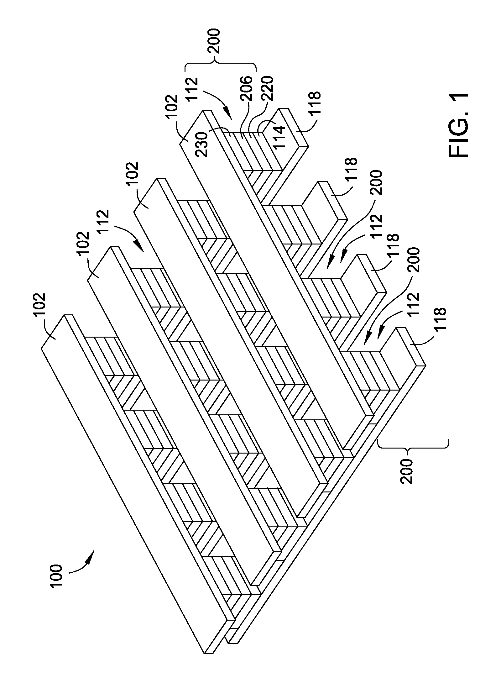
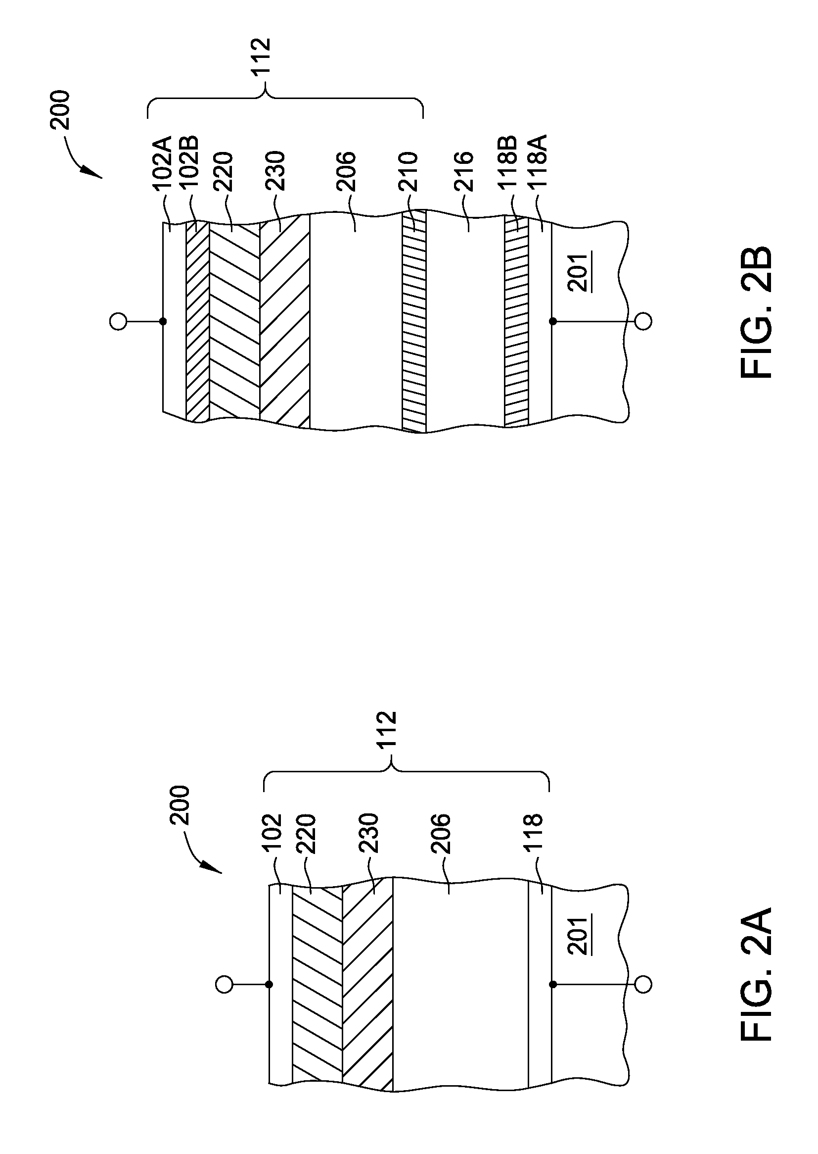
[0124]In accordance with one or more embodiments of the invention, a process of forming the memory device 200 includes forming a resistive switching memory element 112 having an intermediate electrode layer 210 comprising an n-doped polysilicon layer, a variable resistance layer 206 that is about 50 Å thick and comprises hafnium oxide (HfxOy), a current-reducing layer 230 that comprises aluminum doped hafnium oxide (doped HfxOy) at a thickness of between about 5 Å thick about 20 Å thick with a resistivity of about 2 Ω-cm and a current-limiting layer 220 that comprises hafnium nitride (HfxNy) at a thickness of between about 50 Å and 200 Å with a resistivity of between about 10 Ω-cm and an electrode 102 that comprises a layer of titanium nitride (TiN). After forming the memory device 200, optionally at least one thermal processing step is performed to activate the materials within layers and enhance adhesion between the layers.

[0125]In another example of a memory device 200, the resis...


PUM


Abstract

A current-limiting layer and a current-reducing layer are incorporated into a resistive switching memory device to form memory arrays. The incorporated current-limiting layer reduces the occurrence of current spikes during the programming of the resistive switching memory device and the incorporated current-reducing layer minimizes the overall current levels that can flow through the resistive switching memory device. Together, the two incorporated layers help improve device performance and lifetime.

Description

CROSS-REFERENCE TO RELATED APPLICATIONS[0001]This application is a continuation-in-part of co-pending U.S. patent application Ser. No. 13 / 228,744, filed Sep. 9, 2011, and a continuation-in-part of co-pending U.S. patent application Ser. No. 13 / 353,000, filed Jan. 18, 2012, which claims benefit of U.S. provisional patent application Ser. No. 61 / 513,355, filed Jul. 29, 2011. Each of the aforementioned related patent applications is herein incorporated by reference.BACKGROUND OF THE INVENTION[0002]1. Field of the Invention[0003]This invention relates to the formation of resistive switching memory devices.[0004]2. Description of the Related Art[0005]Nonvolatile memory devices are used in systems in which persistent storage is required. For example, nonvolatile memory cards are used in digital cameras to store images and in digital music players to store audio data. Nonvolatile memory devices are also used to persistently store data in computer environments.[0006]Electrically-erasable pr...

Claims


Application Information

Patent Timeline
IPC IPC(8): H01L45/00
CPCH01L45/1233H01L45/146H01L27/2463H01L45/08H01L45/12H01L45/1616G11C13/00H01L27/2409H01L45/145H01L45/1608G11C13/0007G11C2213/72G11C11/00H01L45/1641H10B63/20H10B63/80H10N70/801H10N70/24H10N70/023H10N70/041H10N70/8833H10N70/826H10N70/883H10N70/021
Inventor WANG, YUNCHIANG, TONY P.HASHIM, IMRAN
Owner SANDISK TECH LLC
Why Eureka
Try Eureka