Information processing system including semiconductor device having self-refresh mode

a technology of information processing system and self-refresh mode, which is applied in the field of information processing system, can solve the problems of power consumption of the entire system becoming quite low, inability to use impedance control signals, and power consumption being higher in power-down mode than in self-refresh mod

Active Publication Date: 2013-01-31
LONGITUDE LICENSING LTD
View PDF4 Cites 46 Cited by
  • Summary
  • Abstract
  • Description
  • Claims
  • Application Information

AI Technical Summary

Benefits of technology

[0015]According to the present invention, an impedance of the data terminal can be controlled in response to the impedance control command even in the self-refresh mode.

Problems solved by technology

Accordingly, when the semiconductor device has entered the self-refresh mode, entire power consumption of the system becomes quite low.
However, because the impedance control signal is introduced inside of the DRAM in synchronism with an external clock signal, there is a problem that the impedance control signal cannot be used during a period when the semiconductor device has entered a self-refresh mode in which an input first-stage circuit such as a clock receiver is inactivated.
Therefore, the controller has no alternative but to enter a power-down mode in which the ODT function can be used; however, power consumption is higher in the power-down mode than in the self-refresh mode.
Furthermore, because a clock receiver is always activated in the DRAM described in Japanese Patent Application Laid-open No. 2001-332086, power consumption of the clock receiver cannot be reduced even when the semiconductor device enters the self-refresh mode.
This problem occurs not only in the DRAM but also in all semiconductor devices with the ODT function or the self-refresh mode.
For example, there is the same problem also in a nonvolatile memory, a controller thereof, and a system, which are required to operate at high frequency.
Further, there is the same problem also in a semiconductor device that in a part includes nonvolatile memory cells having a problem of cell data retention.

Method used


Image

  • Information processing system including semiconductor device having self-refresh mode
  • Information processing system including semiconductor device having self-refresh mode
  • Information processing system including semiconductor device having self-refresh mode

Examples


first embodiment

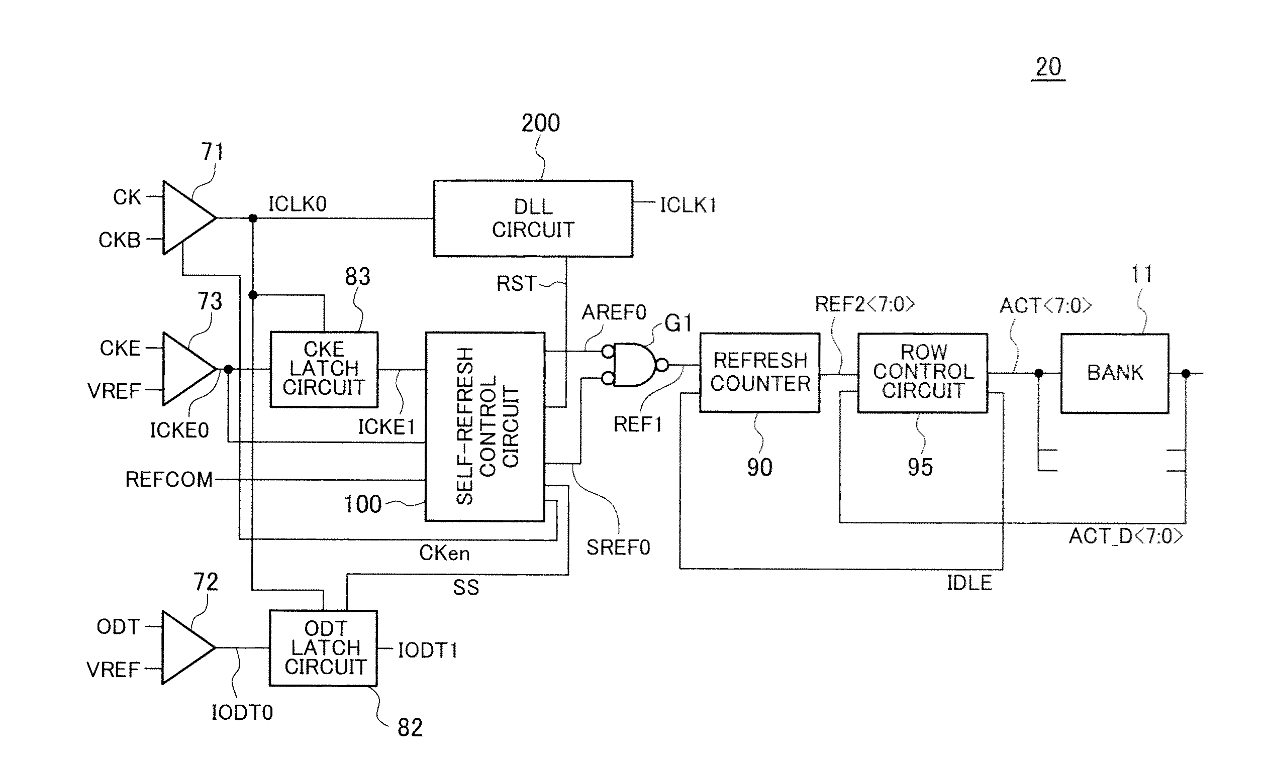
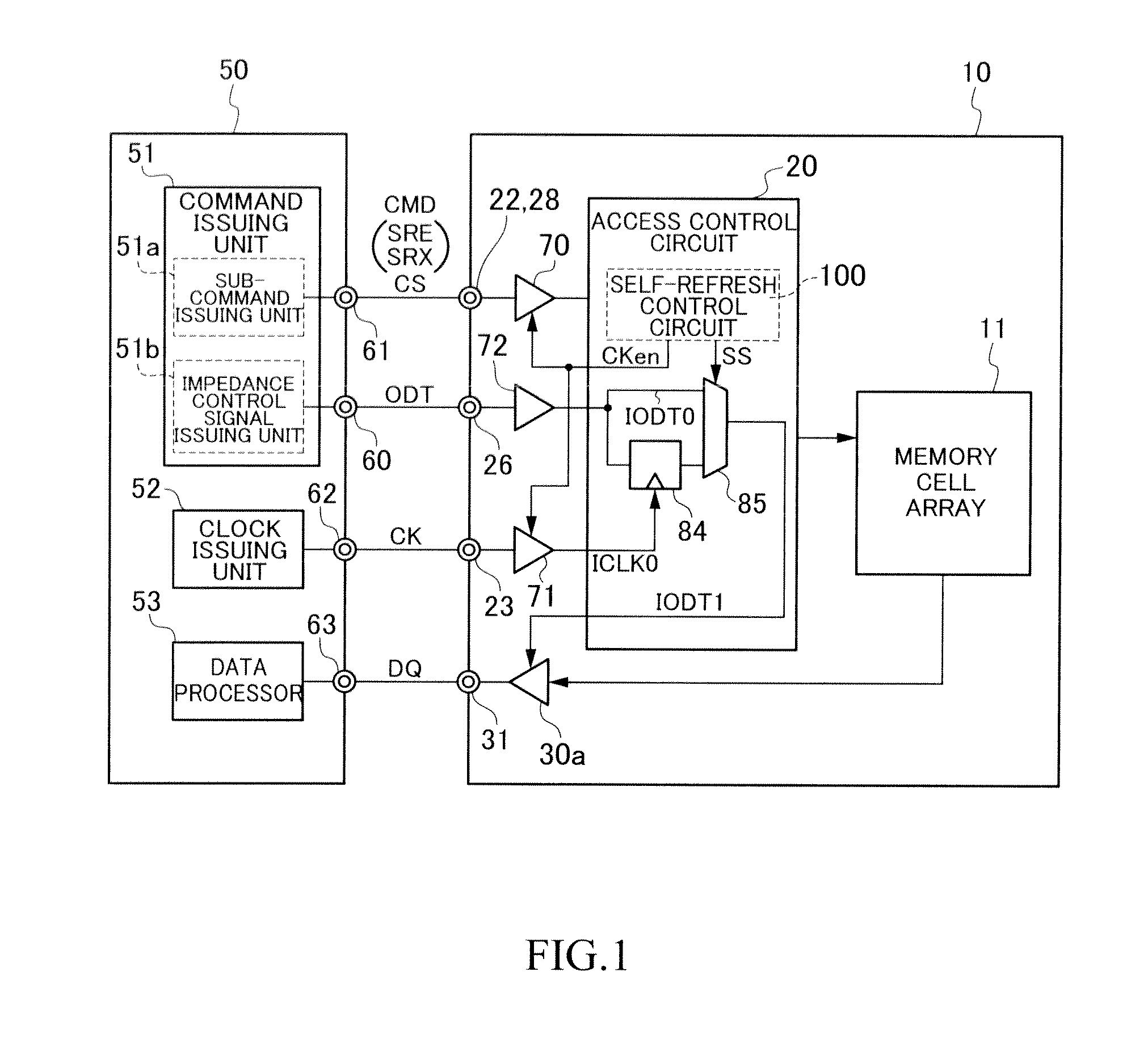
[0062]Turning to FIG. 3, the access control circuit 0 includes input buffer circuits 71 to 73. The input buffer circuit 71 receives the external clock signals CK and CKB and generates the internal clock signal ICLK0, and is also referred to as “first input buffer circuit” in the present invention. The input buffer circuit 72 receives the impedance control signal ODT and generates an impedance control signal IODT0, and is also referred to as “second input buffer circuit” in the present invention. The input buffer circuit 73 receives the clock enable signal CKE and generates a clock enable signal ICKE0, and is also referred to as “third input buffer circuit” in the present invention. The input buffer circuit 71 is activated or inactivated according to an enable signal CKen. The input buffer circuit 71 is activated when the enable signal CKen is high. On the other hand, the input buffer circuits 72 and 73 are always activated. This is because, in the first embodiment, the impedance con...

third embodiment

[0103]When the self-refresh command SRE is issued at the time t32, the SR latch circuit L1 shown in FIG. 6 is set and the enable signal CKen is changed to a low level. This inactivates the input buffer circuits 71 and 72a shown in FIG. 10 and reduces power consumption. The impedance control signal CDT cannot be input during a period when the semiconductor device has entered the self-refresh mode. In FIG. 11, the periods in which input of the impedance control signal ODT is ineffective (Don't care) are shown by hatching. In the example shown in FIG. 11, the impedance control signal ODT is not input (that is, Don't care) in most of the period when the semiconductor device 10 is in the self-refresh mode. The impedance control signal ODT cannot be supplied from the controller 50 in most of the period when the semiconductor device 10 is in the self-refresh mode because the input buffer circuit 72a is inactivated in this period. Specifically, logic of generating the enable signal CKen sho...

fourth embodiment

[0142]the present invention is explained next.

[0143]An access control circuit according to the fourth embodiment has a configuration in which the self-refresh control circuit 100b is replaced by a self-refresh control circuit 100c. Other features of the access control circuit of the fourth embodiment are basically the same as those of the access control circuit 20b shown in FIG. 15.

[0144]Turning to FIG. 18, the self-refresh control circuit 100c is different from the self-refresh control circuit 100b shown in FIG. 16 in that the one-shot pulse generating circuit OP1 is used instead of the oscillator 150. A signal supplied to the set node S of the SR latch circuit L1 is used as it is as the self-refresh signal SREF0. Output from the one-shot pulse generating circuit OP1 is used as the update start signal ST. Other features of the self-refresh control circuit 100a are basically the same as those of the self-refresh control circuit 100b shown in FIG. 16, and therefore like elements are ...


PUM


Abstract

Disclosed herein is a semiconductor device having a self-refresh mode in which a refresh operation of the storage data is performed. The semiconductor device activates an input buffer circuit that receives an impedance control command to control an impedance of the data terminal even in the self-refresh mode so that the semiconductor device can change an impedance of the data terminal during the self-refresh mode.

Description

BACKGROUND OF THE INVENTION[0001]1. Field of the Invention[0002]The present invention relates to an information processing system and a control method thereof, and more particularly to an information processing system including a semiconductor device with a self-refresh mode and a control method thereof. The present invention also relates to a control method of a controller, and more particularly to a controller that controls a semiconductor device with a self-refresh mode and a control method thereof.[0003]2. Description of Related Art[0004]An operation mode called a self-refresh mode is provided for the DRAM. The self-refresh mode is a kind of standby mode in which refresh of storage data included in storage cells is periodically performed inside of the DRAM in asynchronism with outside. A controller can stop issuance of many external signals such as an external clock signal and a command signal to be supplied to the semiconductor device, during a period when the semiconductor dev...

Claims


Application Information

Patent Timeline
Patent Type & Authority Applications(United States)
IPC IPC(8): G11C11/402G11C7/00
CPCG11C11/40615G11C11/4093G11C7/222G06F13/1636G11C7/22G11C2211/4067Y02D10/00G11C7/04
Inventor FUJISAWA, HIROKI
Owner LONGITUDE LICENSING LTD
Why Eureka
Try Eureka