Kit of building blocks for constructing educational electronic circuits

a technology of electronic circuits and building blocks, applied in the field of educational electronic circuits, can solve the problems of inability to equalize or increase the width of the circuit, and achieve the effect of convenient route and more economical

Inactive Publication Date: 2013-01-31
VALBUENA PABLO
View PDF1 Cites 7 Cited by
  • Summary
  • Abstract
  • Description
  • Claims
  • Application Information

AI Technical Summary

Benefits of technology

[0023]Soldering ferromagnetic steel sheets to a PCB is something unknown in the art. The reason is that PCB's are made to develop an electrical function, but not a mechanical function. The copper pads and the copper traces of the PCB's are not designed to withstand tensions, since it could possibly provoke the peeling of the PCB. In brief, the perforated plastic sheet brings the following advantages:
[0024]The tension of the tin solder between the ferromagnetic steel sheet and its copper pad is reduced. Furthermore, the direction of the force that the solder withstands is exerted in the direction parallel to the copper pad and not in the perpendicular direction.
[0025]The tension of the union between the substrate of the board and the copper pad is reduced. Furthermore, the force that the union withstands is parallel to the surface of the copper pad and not perpendicular. That way the peeling of the PCB is prevented.
[0028]Due to the previous advantages and also due to the fact that the present contact plates and electronic components are smaller, it is possible to use thinner PCB's than with the known systems. It is possible to use PCB's of 0.8 mm thick instead of the more common 1.6 mm thick PCB's. Thin PCB's are more economical and easier to route, to mechanize.

Problems solved by technology

One limitation of the size of the magnets is that its width cannot be equal or bigger than the grid distance to avoid that two adjacent magnets make contact.

Method used


Image

  • Kit of building blocks for constructing educational electronic circuits
  • Kit of building blocks for constructing educational electronic circuits
  • Kit of building blocks for constructing educational electronic circuits

Examples


fourth embodiment

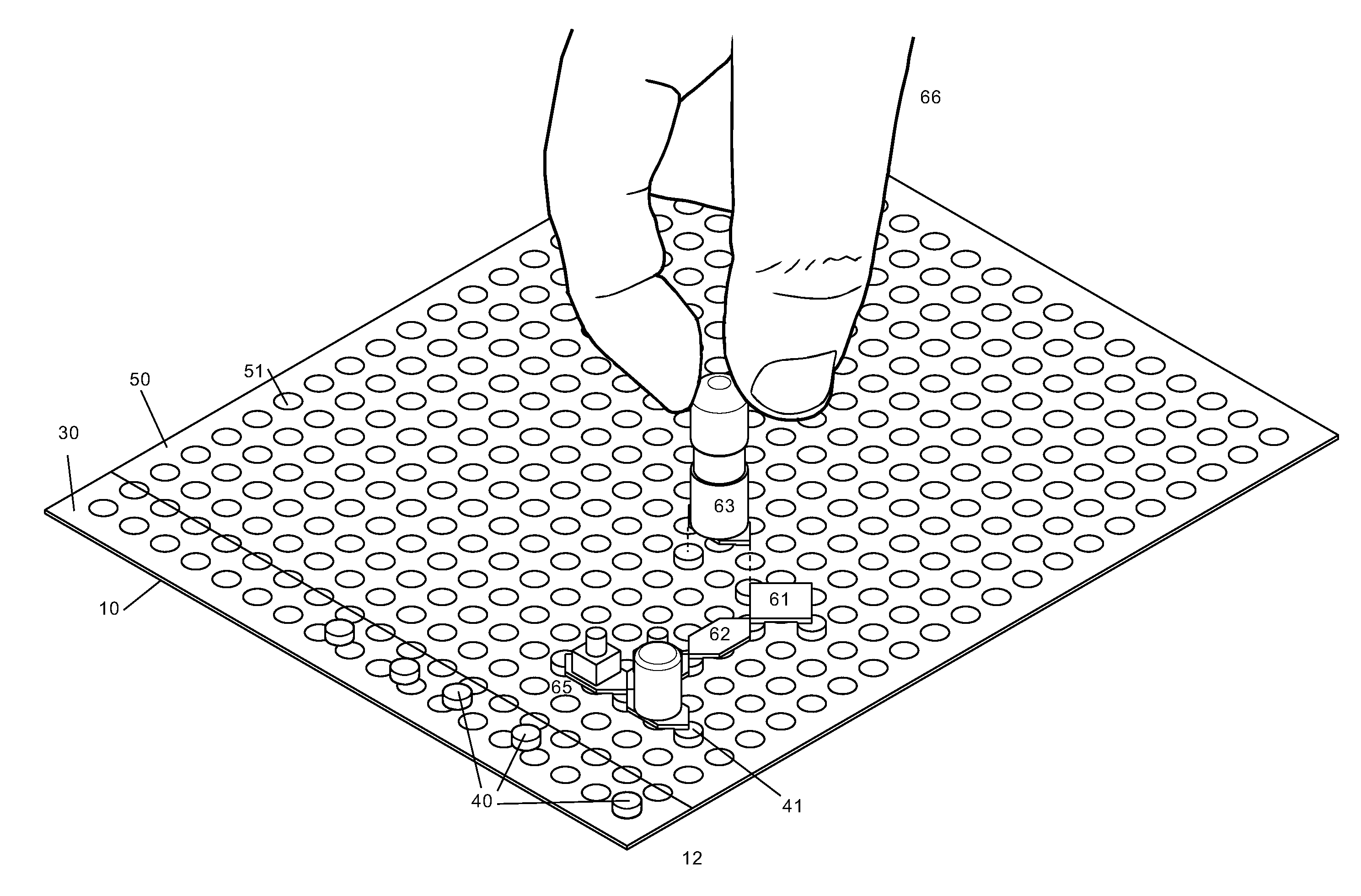
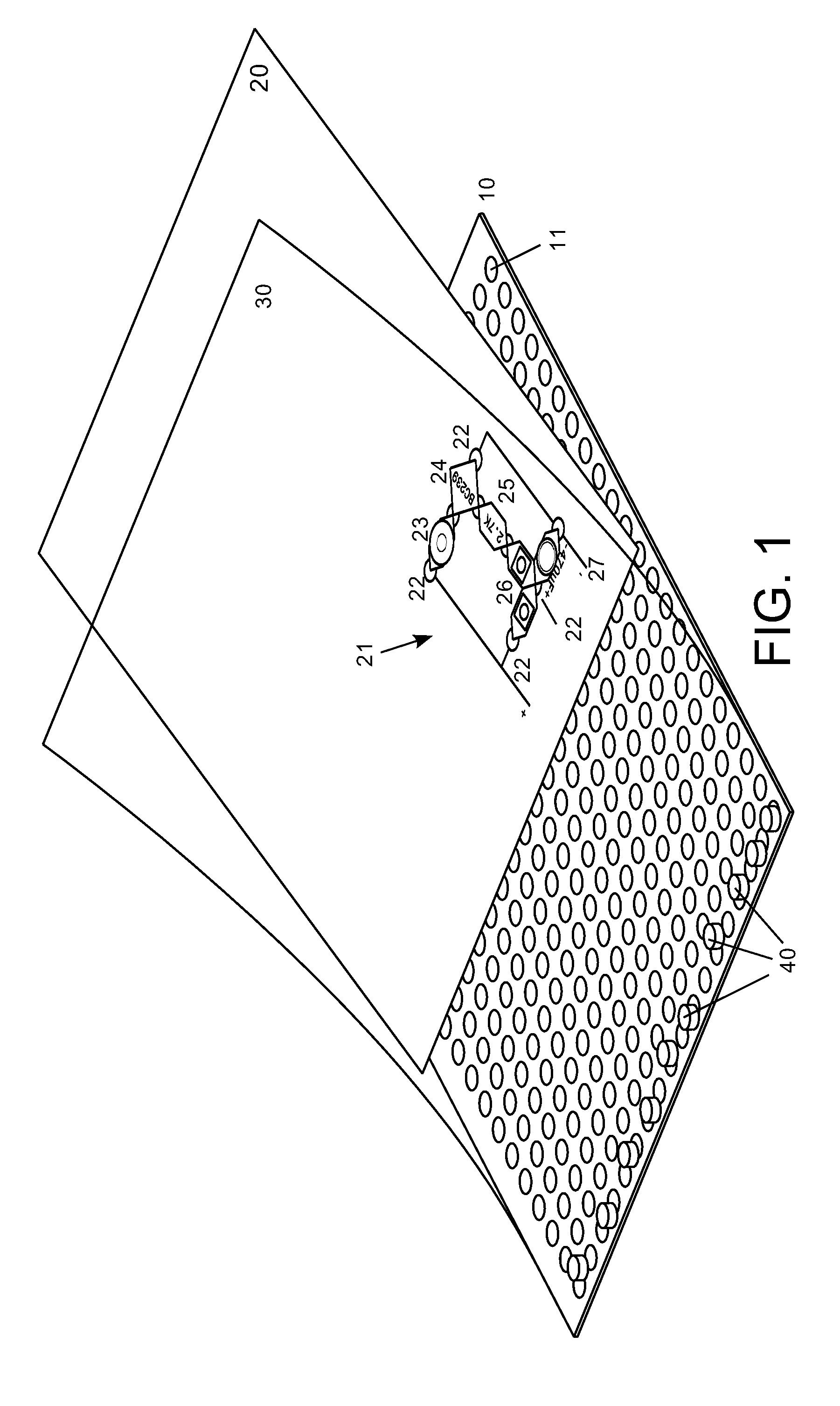
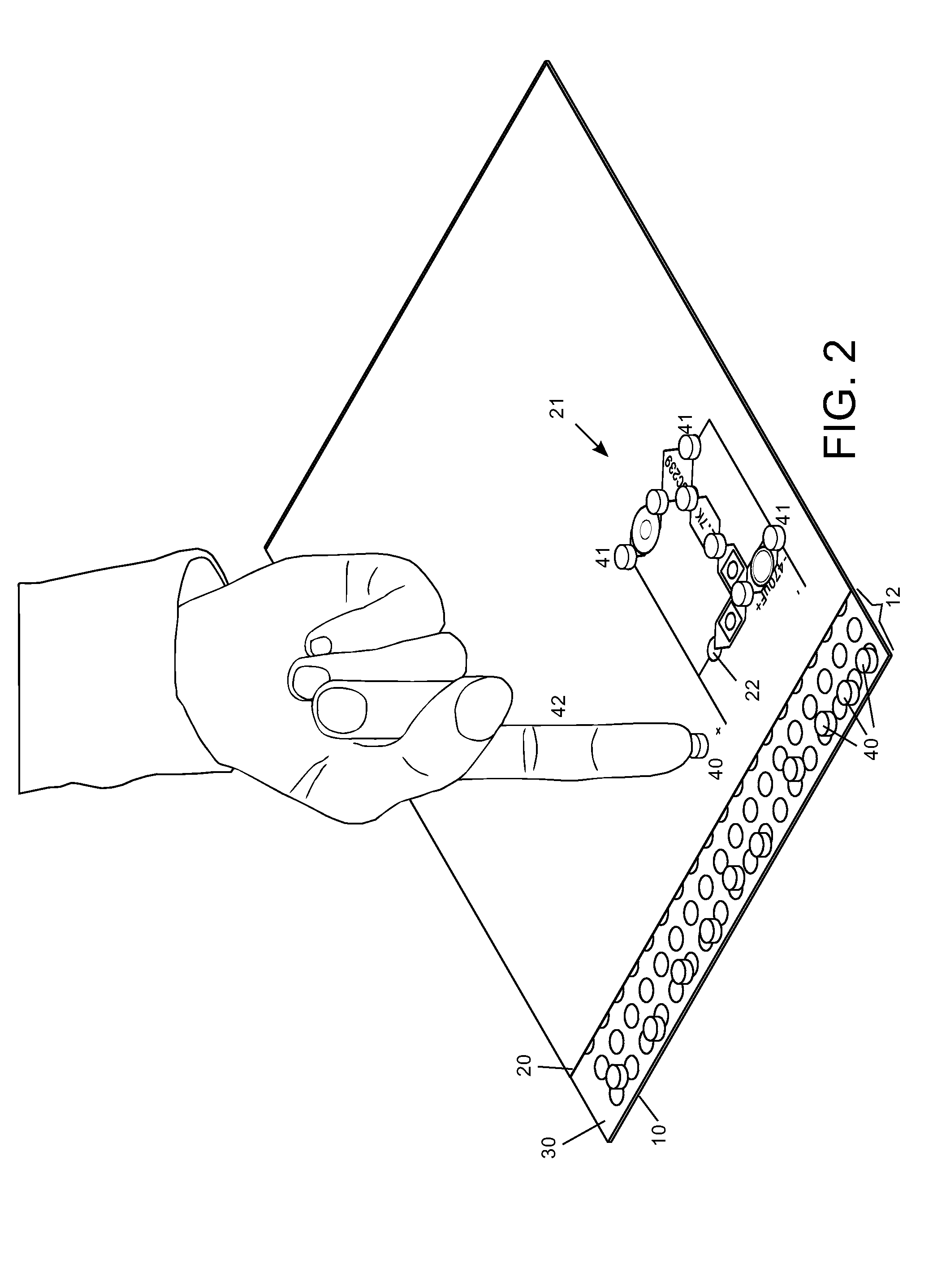
[0096]FIG. 25A and FIG. 25B show the invention. In this embodiment the building block 75 is based on a single-sided PCB 750. The PCB 750 has plated through-holes 7053 to insert and solder the pins or the leads 7051 of an electronic component 705 that is not an SMD component.

[0097]FIG. 25B shows the lower side of the block 75. On that side can be seen the copper pads 7054 and copper traces to be placed in position by soldering the steel sheet plates 702. The figure also shows the tin meniscus 7052 that makes the joint between the lead and the copper pad.

[0098]FIGS. 26A, 26B and 26C show another embodiment of the invention. The building blocks 81 have as its base a double-sided PCB. FIG. 26A shows the upper face of the PCB 810. On the upper side of the PCB is soldered the SMD electronic component 701 that communicates through two vias 811 with the lower side.

[0099]FIG. 26B shows the reverse of the building block of FIG. 26A. FIG. 26C is an exploded view of FIG. 26B and shows the via h...

embodiment 85

[0104]FIGS. 27A, 27B and 27C show a different embodiment of the invention with contact plates that overhang from the PCB. The building blocks of this embodiment 85 are very similar to the aforementioned blocks 81. The main difference is that the electronic components have leads or pins. These figures show a component 705 with two leads 7051. The leads are inserted and soldered to the plated through-holes of the PCB. The steel sheets have a hole 852 to let the pins or the leads pass through. These holes are slightly bigger than the tin meniscus 7052. For the same reason, the retaining stops 813 exhibit now a small recess 853.

[0105]FIGS. 28A to 29E show different jumpers. The jumpers are used to connect electrically two or more points of the grid of contacts, i.e. two or more magnets. The simplest jumper considered is a ferromagnetic steel sheet. For example, FIG. 29A shows a square steel sheet 802 to connect two adjacent magnets. This kind of jumpers feels disarranging forces and for...


PUM


Abstract

Kit of building blocks for constructing educational electronic circuits comprising a ferromagnetic base plate (10) with the diagram (21) of the circuit to construct. A transparent plastic sheet (30) covers the diagram. A group of magnets (40, 41) rest on the plastic sheet attracted by the plate (10). The surface of the magnets (40, 41) is electrically conducting. A plurality of building blocks can be detachably mounted on the magnets (40, 41), each magnet (41) connecting the steel sheets (702) of the building blocks that rest on it. The steel sheets of the blocks are designed so that the attraction forces that arise between the magnets and the sheets drive the modules exactly to a desired equilibrium position.

Description

1. FIELD OF TECHNOLOGY[0001]The kit that is presented forms part of educational games that physically and actually construct electronic circuits from interchangeable electronic modular elements. These units are joined together over a base panel that serves as support to the whole unit. The systems mentioned are clearly differentiated from other educational systems which use a computer to simulate circuits.2. BACKGROUND ART[0002]Several systems are known in the art for learning electronics by setting-up circuits; below can be found a classification of the most important ones following the excellent topological analysis made by Mr. Reinhard Niehoff in his website (http: / / erinacom.org / elektronik / index.html, or http: / / web.archive.org / web / 20071017020557 / erinacom.de / elektronik / system / schaltung / schaltung.html).2.1. Classification of the Known Systems[0003]2.1.1. Systems in which the Connections Among Elements is Done through Cables (Verdrahtungssysteme in German).[0004]In these systems the...

Claims


Application Information

Patent Timeline
Patent Type & Authority Applications(United States)
IPC IPC(8): G09B23/18
CPCG09B23/185G09B23/183
Inventor VALBUENA VAZQUEZ, PABLO
Owner VALBUENA PABLO
Why Eureka
Try Eureka