Laminated inductor

a technology of inductor and inductor body, which is applied in the direction of transformer/inductance details, coils, inductances, etc., can solve the problems of substantially lower volume resistivity of materials compared to conventional ferrite, and achieve the improvement of the l value of the inductor, shortening/breaking easily, and improving the overall magnetic permeability of the devi

Active Publication Date: 2013-02-07
TAIYO YUDEN KK
View PDF6 Cites 38 Cited by
  • Summary
  • Abstract
  • Description
  • Claims
  • Application Information

AI Technical Summary

Benefits of technology

[0014]According to the present invention, soft magnetic alloy grains of a large grain size are used for the cover regions, so the magnetic permeability of the device as a whole improves and the L value of the inductor also improves as a result. On the other hand, soft magnetic alloy grains of a small grain size are used for the magnetic part in the internal conductive wire forming region, so the internal conductive wires do not short / break easily and the device can be made smaller as a result. Since the soft magnetic alloy grains for the top and bottom cover regions can be constituted by a soft magnetic alloy whose composition is the same as or similar to that of the soft magnetic alloy grains for the magnetic part in the internal conductive wire forming region, the bonding property of the top and bottom cover regions with the internal conductive wire forming region improves, which in turn helps improve the strength of the device as a whole.
[0015]According to a favorable embodiment of the present invention, use of a Fe—Cr—Si alloy for the soft magnetic alloy allows the top and bottom cover regions, and magnetic part in the internal conductive wire forming region, to be made denser and consequently the strength of the laminated inductor as a whole improves.

Problems solved by technology

On the other hand, these materials have a substantially lower volume resistivity compared to conventional ferrite.

Method used


Image

  • Laminated inductor
  • Laminated inductor
  • Laminated inductor

Examples


example

[0059]The present invention is explained more specifically below using examples. Note, however, that the present invention is not at all limited to the embodiments described in these examples.

[0060][Specific Structure of Laminated Inductor]

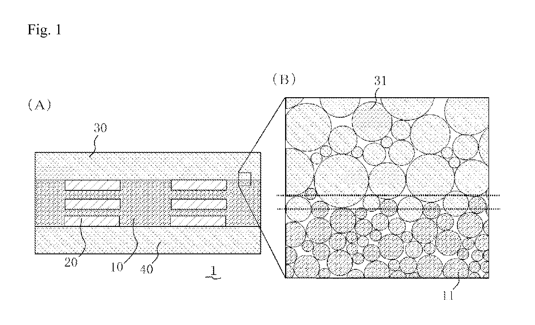
[0061]An example of the specific structure of the laminated inductor 1 manufactured in this example is explained. As a component, the laminated inductor 1 has a length of approx. 3.2 mm, width of approx. 1.6 mm and height of approx. 1.0 mm, and has a rectangular solid shape as a whole.

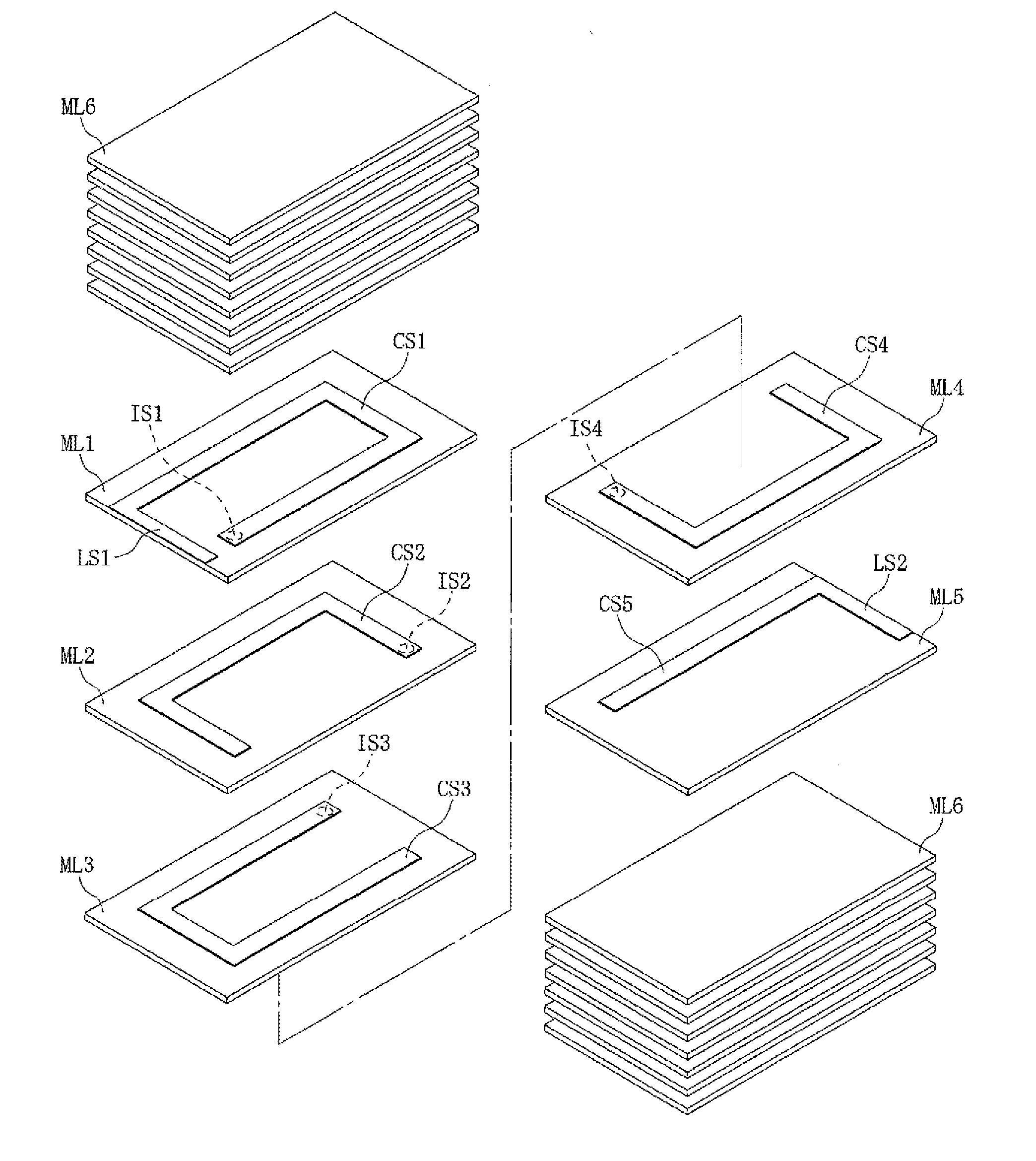
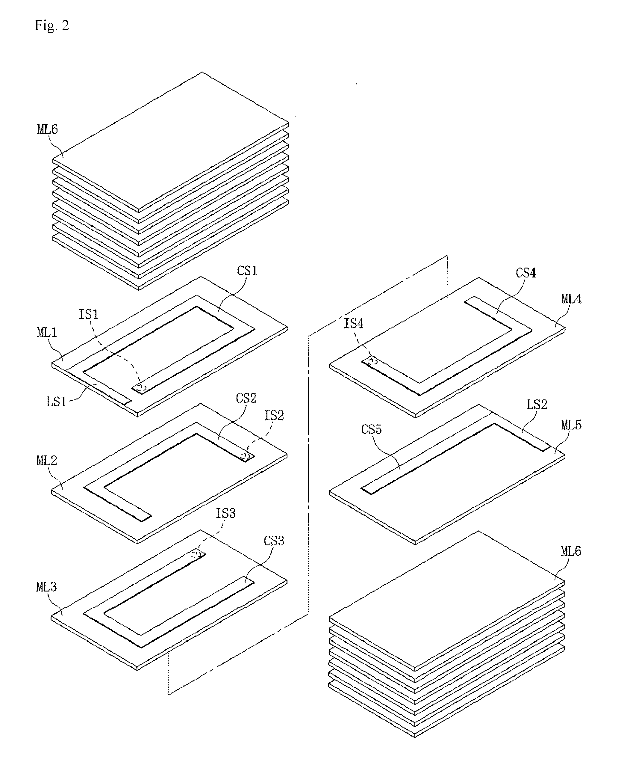
[0062]FIG. 2 is a schematic exploded view of a laminated inductor. The magnetic part 10 in the internal conductive wire forming region has a structure whereby a total of five magnetic layers ML1 to ML5 are integrated together. The top cover region 30 has a structure whereby eight layers of magnetic layer ML6 are integrated together. The bottom cover region 40 has a structure whereby seven layers of magnetic layer ML6 are integrated together. The laminated inductor 1 ...


PUM

PropertyMeasurementUnit
grain sizeaaaaaaaaaa

Abstract

A laminated inductor having an internal conductive wire forming region, as well as a top cover region and bottom cover region formed in a manner sandwiching the internal conductive wire forming region between top and bottom; wherein the internal conductive wire forming region has a magnetic part formed with soft magnetic alloy grains, as well as helical internal conductive wires embedded in the magnetic part and constituted by a conductor; and at least one of the top cover region and bottom cover region (or preferably both) is/are formed with soft magnetic alloy grains whose constituent elements are of the same types as those of, and whose average grain size is greater than that of, the soft magnetic alloy grains constituting the magnetic part in the internal conductive wire forming region.

Description

BACKGROUND[0001]1. Field of the Invention[0002]The present invention relates to a laminated inductor.[0003]2. Description of the Related Art[0004]A method of manufacturing a laminated inductor has been traditionally known, which comprises printing internal conductor patterns on ceramic green sheets containing ferrite, etc., and then stacking the sheets on top of one another and sintering the stacked sheets.[0005]According to Patent Literature 1, through holes are formed at specified positions in a ceramic green sheet made with ferrite powder. Next, on one main side of the sheet in which through holes have been formed, a coil conductor pattern (internal conductor pattern) is printed using a conductive paste in such a way that when a multiple number of the sheets are stacked and their through holes connected, a helical coil will be formed.[0006]Next, the above sheets having through holes and coil conductor pattern formed in / on them are stacked on top of one another according to a spec...

Claims


Application Information

Patent Timeline
Patent Type & Authority Applications(United States)
IPC IPC(8): H01F27/02
CPCH01F17/0033H01F17/0013H01F17/00H01F27/28
Inventor MATSUURA, HITOSHIARAI, TAKAYUKIOTAKE, KENJI
Owner TAIYO YUDEN KK
Why Eureka
Try Eureka