Thin film transistor, method fabricating thereof, liquid crystal display device and method for fabricating the same

a thin film transistor and liquid crystal display technology, applied in transistors, optics, instruments, etc., can solve the problems of reducing the aperture ratio of the liquid crystal display, and achieve the effects of reducing product cost consumed, reducing failures, and being easy to carry ou

Active Publication Date: 2013-02-14
LG DISPLAY CO LTD
View PDF2 Cites 13 Cited by
  • Summary
  • Abstract
  • Description
  • Claims
  • Application Information

AI Technical Summary

Benefits of technology

[0029]According to a thin-film transistor, a fabrication method thereof, a liquid crystal display device using the same, and a fabrication method thereof in accordance with the present invention, it is possible to reduce failures occurred during the formation of a gate insulating layer that has been a problem in the related art. In particular, in the related art, a gate electrode is formed in a thick manner, thus causing a phenomenon that a lateral surface of the gate electrode is exposed during the etching process or data is open, but according to the present invention, a lateral surface of the gate electrode is covered in a thick manner and a step height due to a thickness of the gate electrode can be reduced by the formation of a planarized insulating layer, thus preventing a phenomenon that a lateral surface of the gate electrode is exposed during the etching process or data is open in the related art.
[0030]Furthermore, according to a thin-film transistor, a fabrication method thereof, a liquid crystal display device using the same, and a fabrication method thereof in accordance with the present invention, processes formed with a thick layer can be easily carried out due to the formation of an interlayer insulating layer. In other words, a gate insulating layer formed subsequent to the interlayer insulating layer may be formed with no large curvature, thereby facilitating the deposition of other subsequently formed elements. It has an effect of reducing product cost consumed during the implementation of an ultra dimension (UD) product.
[0031]In addition, according to a thin-film transistor, a fabrication method thereof, a liquid crystal display device using the same, and a fabrication method thereof in accordance with the present invention, metal patterns including a gate electrode can be implemented in the form of a narrow and thick shape rather than in the form of a thin and wide area to increase the transmittance in case of a liquid crystal display, thereby reducing the cost incurred during the fabrication of a backlight unit.

Problems solved by technology

However, the enlarged area of the gate electrode causes a reduced aperture ratio of the liquid crystal display, and thus studies have been carried out in the direction of increasing a thickness of the gate electrode rather than enlarging an area of the gate electrode.

Method used


Image

  • Thin film transistor, method fabricating thereof, liquid crystal display device and method for fabricating the same
  • Thin film transistor, method fabricating thereof, liquid crystal display device and method for fabricating the same
  • Thin film transistor, method fabricating thereof, liquid crystal display device and method for fabricating the same

Examples


Embodiment Construction

[0042]Hereinafter, the structure of a thin-film transistor according to a preferred embodiment of the present invention will be described in detail with reference to the accompanying drawings. Even in different embodiments according to the present disclosure, the same or similar reference numerals are designated to the same or similar configurations, and the description thereof will be substituted by the earlier description.

[0043]Unless clearly used otherwise, expressions in the singular number used in the present disclosure may include a plural meaning.

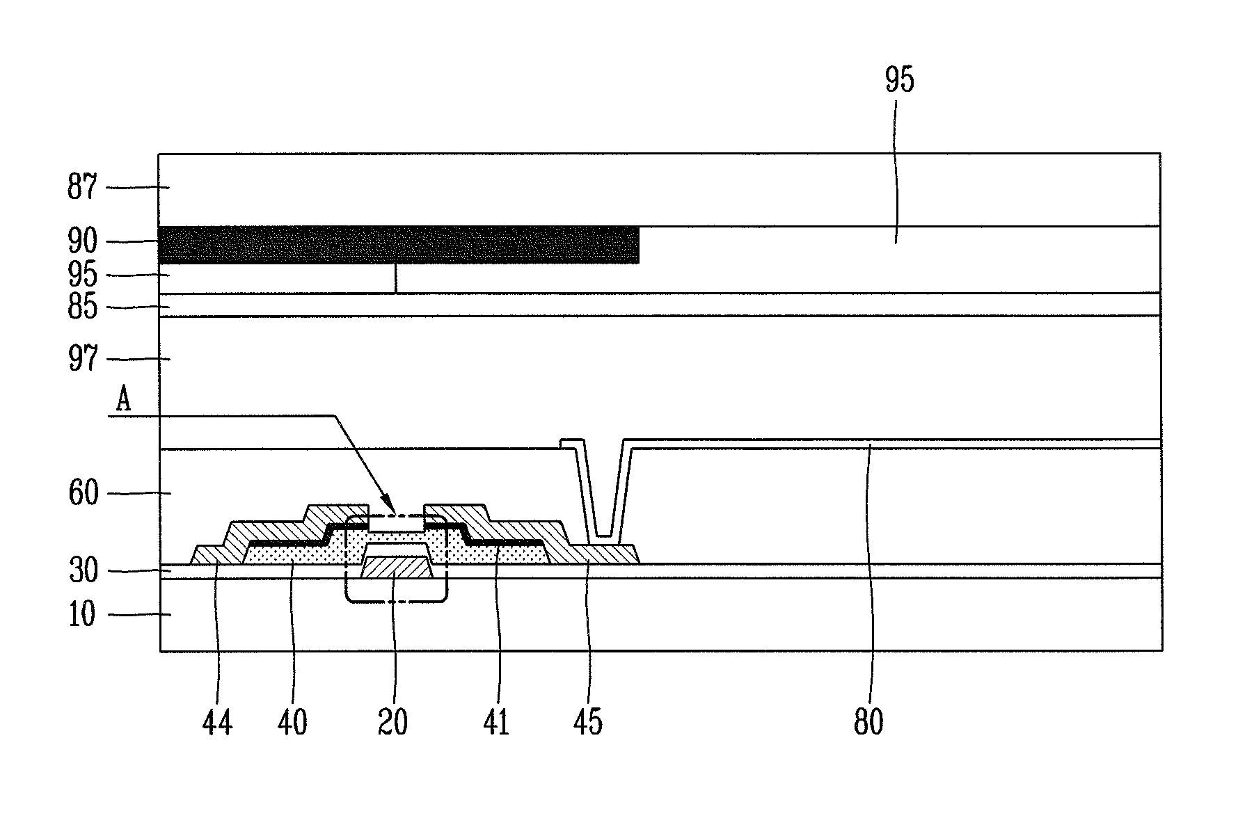
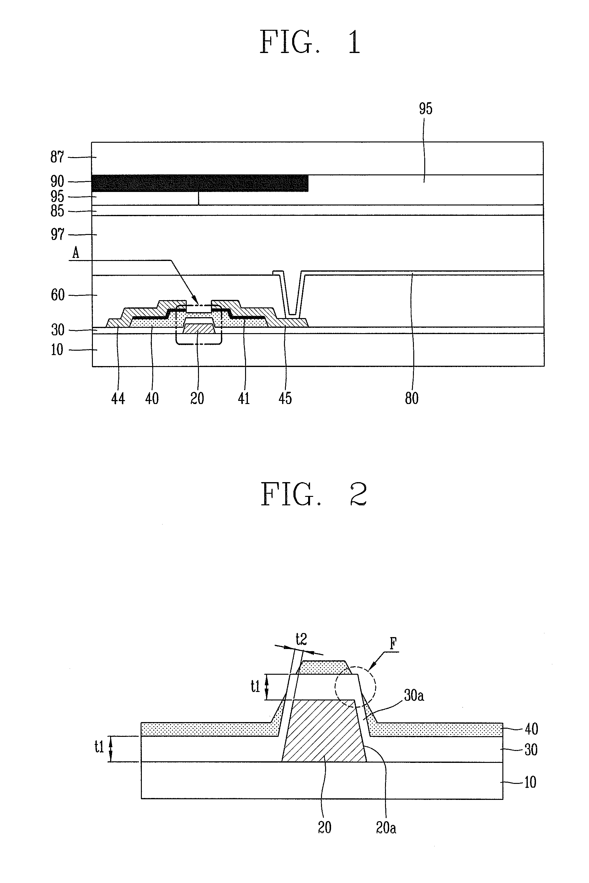
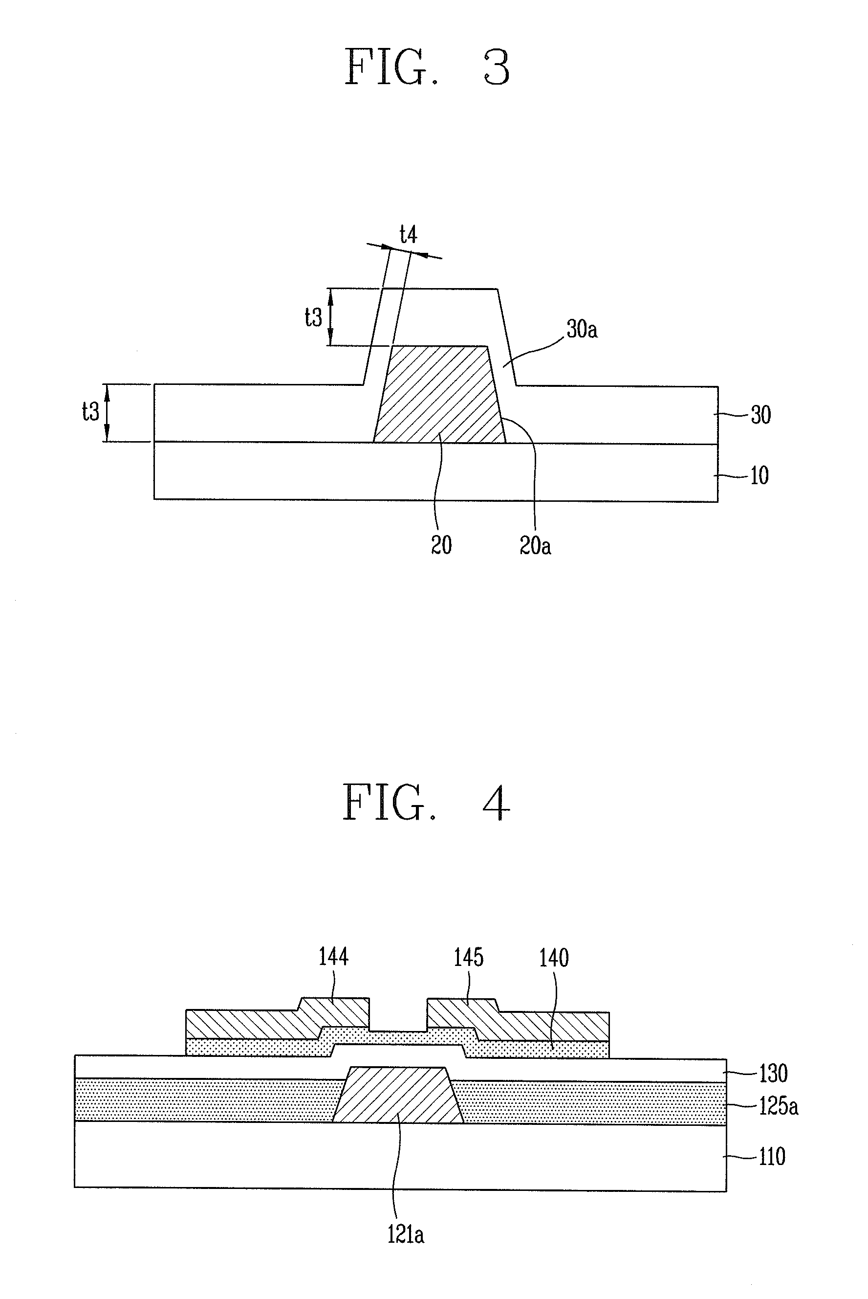
[0044]FIG. 4 is a view schematically illustrating the cross-sectional structure of a thin-film transistor according to the present invention. A thin-film transistor according to the present invention may include a substrate 110, a gate electrode 121a formed on the substrate 110, a planarized insulating layer 125a formed at a lateral surface portion of the gate electrode 110 and at an upper portion of the substrate 110, a gate insulat...


PUM


Abstract

A thin-film transistor array substrate and a fabrication method thereof according to an embodiment of the present invention are disclosed to form an interlayer insulating layer, thereby reducing a failure occurred during the process subsequent to a gate electrode. The thin-film transistor disclosed according to the present invention may include a substrate, a gate electrode formed on the substrate, a planarized insulating layer formed at a lateral surface portion of the gate electrode and at an upper portion of the substrate, a gate insulating layer formed on the planarized insulating layer containing an upper portion of the gate electrode, an active layer formed at an upper portion of the planarized insulating layer located at an upper side of the gate electrode, and a source electrode and a drain electrode formed on the active layer and separated from each other based on a channel region.

Description

CROSS-REFERENCE TO RELATED APPLICATIONS[0001]This application claims the benefit of Korean Patent Application No. 10-2011-0079281, filed on Aug. 9, 2011, which is hereby incorporated by reference for all purposes as if fully set forth herein.BACKGROUND OF THE INVENTION[0002]1. Field of the Invention[0003]The present invention relates to a thin-film transistor and a liquid crystal display device, and more particularly, to a thin-film transistor, a fabrication method thereof, a liquid crystal display device using the same, and a fabrication method thereof.[0004]2. Description of the Related Art[0005]In recent years, with rising interests in information displays and increasing demands to use portable information media, researches and commercialization of light-weight and thin-profile flat panel displays (FPDs) for substituting traditional displays such as cathode ray tubes (CRTs) have been actively carried out. In particular, among those flat panel displays, a liquid crystal display (L...

Claims


Application Information

Patent Timeline
Patent Type & Authority Applications(United States)
IPC IPC(8): H01L29/786H01L33/08H01L21/336
CPCH01L21/28008H01L29/78636H01L27/1244G02F2001/133357H01L27/1288G02F1/136286G02F1/1368H01L27/1248G02F1/133357H01L29/78606
Inventor OH, TAE-YOUNGCHO, HEUNG-LYULJUNG, JI-EUN
Owner LG DISPLAY CO LTD
Why Eureka
Try Eureka