Device for Electric Insulation of a Conducting Plane

a technology of conducting plane and electric insulation, which is applied in the direction of electrical apparatus contruction details, semiconductor/solid-state device details, printed circuit non-printed electric components association, etc., can solve the problems of increasing the heat resistance of the substrate and increasing their temperature, so as to increase the heat resistance of the substrate and reduce the effect of cooling

Active Publication Date: 2013-02-21
ALSTOM TRANSPORT TECH SAS
View PDF13 Cites 1 Cited by
  • Summary
  • Abstract
  • Description
  • Claims
  • Application Information

AI Technical Summary

Benefits of technology

[0005]However, the increase in the thickness of the insulating substrate in order to have a higher breakdown voltage causes an increase in the heat resistance...

Problems solved by technology

However, the increase in the thickness of the insulating substrate in order to have a higher breakdown voltage causes an increase in the heat resistance of...

Method used


Image

  • Device for Electric Insulation of a Conducting Plane
  • Device for Electric Insulation of a Conducting Plane
  • Device for Electric Insulation of a Conducting Plane

Examples


second embodiment

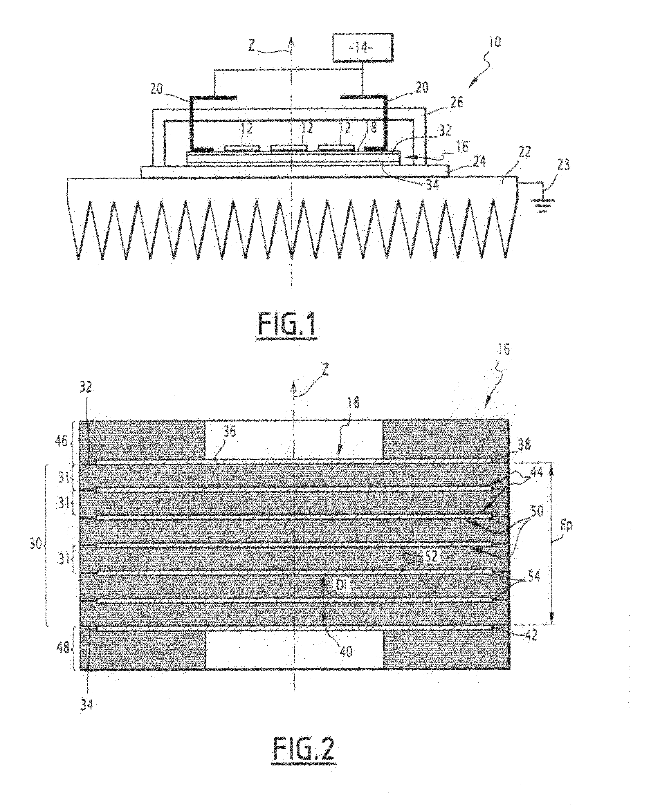
[0063] each conducting area 50 includes a guard ring 60 and an electrically conducting intermediate layer 62 positioned in the insulating substrate 30 parallel to the first outer layer 36. Each conducting area 50 also includes a link 64 for connecting the guard ring 60 to the corresponding intermediate layer 62.

[0064]In the exemplary embodiment of FIG. 4, the number N of conducting areas 50 is equal to 5.

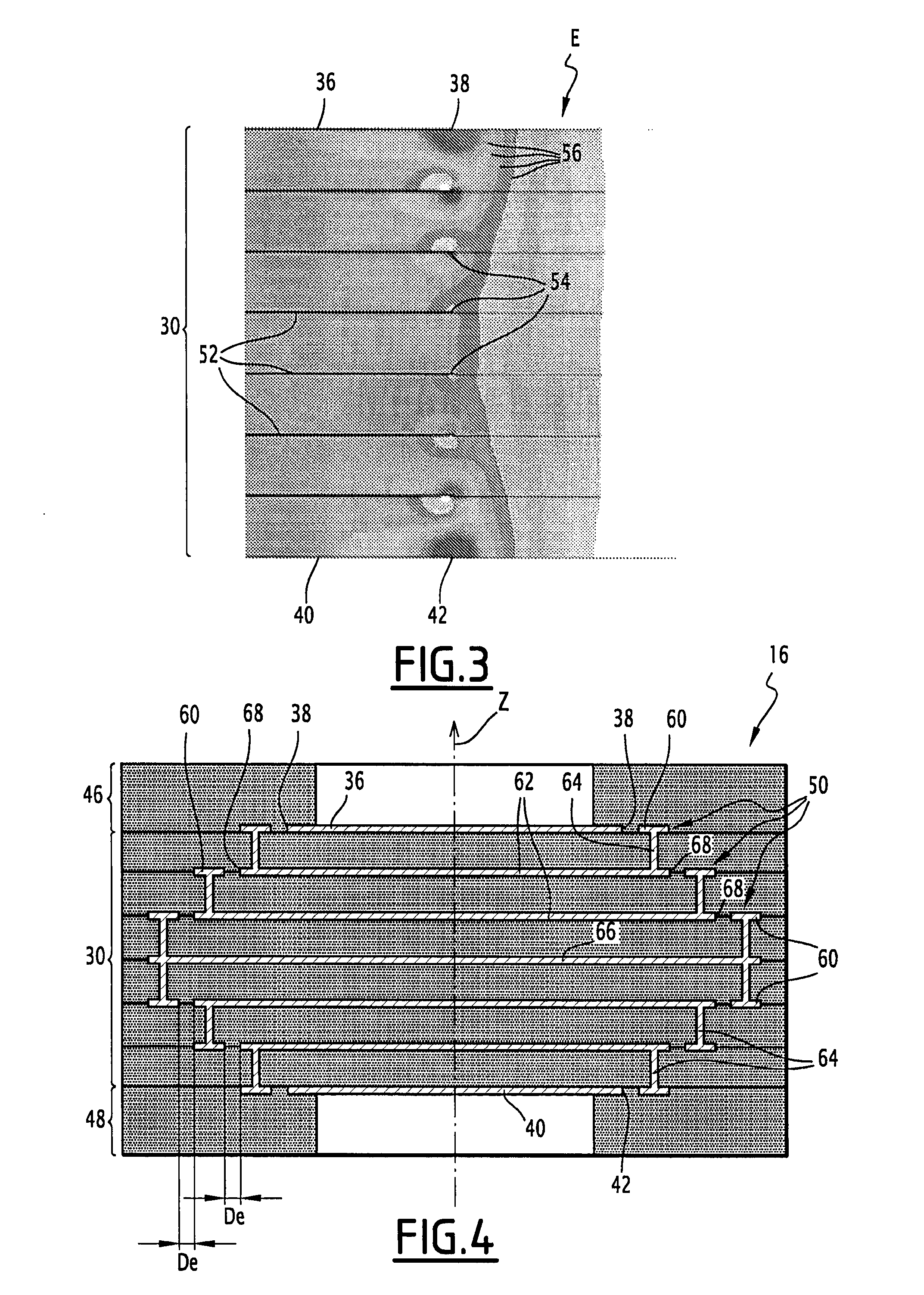
[0065]In the following of the description, a guard ring designates a conducting portion surrounding a conducting layer, the guard ring not necessarily being in the shape of a circular ring. In the exemplary embodiments of FIGS. 4 to 8, the guard rings 60 are of a square shape with rounded angles, the conducting layers being square-shaped. Each guard ring 60 is obtained by metallization of a corresponding insulating stratum 31 of the insulating substrate. Each guard ring 60 is for example made in tungsten or in molybdenum.

[0066]A guard ring 60 is positioned in the plane of each condu...

first embodiment

[0069]Thus, each conducting area 50 gives the possibility of imposing an electric potential of constant value and distinct from that of the other areas 50, the value of the electric potential of a corresponding conducting area being determined by the value of the electric potential of the intermediate layer 62 of the conducting area in the vicinity of the middle axis Z by means of the formula (2) described earlier for the

[0070]The values of the electric potentials Vi of the conducting areas 50 decrease from the edge 38 of the first outer layer 36 towards the outside of the device 16 and towards the second outer layer 40.

[0071]The operation of this second embodiment is like the one of the first embodiment, the conducting areas 50 allowing the potential lines to be moved apart from each other as compared with an electric insulation device of the state of the art only including the outer conducting layers in the absence of any additional conducting area. The value of the electrostatic ...

third embodiment

[0074] each conducting area 50 includes at least one guard ring 60 and an electrically conducting intermediate layer 62 positioned in the insulating substrate 30 parallel to the first outer layer 36. Each conducting area 50 also includes a link 64 for connecting said or each guard ring 60 to the corresponding intermediate layer 62.

[0075]In the exemplary embodiment of FIG. 6, the number N of conducting areas 50 is equal to 5.

[0076]A guard ring 60 is positioned in the plane of each conducting layer 36, 40, 62 except for a central intermediate layer 66 substantially positioned at half the distance between the first and the second outer layer 36, 40. Each intermediate layer 62 has a peripheral edge 68, and the spacing between the peripheral edge 38, 42, 68 of the corresponding conducting layer and the guard ring 60 is for example equal to a predetermined distance De.

[0077]A plurality P of guard rings 60 are positioned in the plane of the outer layers 36, 40, the P guard rings being spac...


PUM


Abstract

A device for insulating an electrically conducting plane having a first electric potential relatively to a second electric potential is provided. The device comprises an insulating substrate including two parallel planar surfaces, and a first conducting outer layer and an electrostatic field reducer. The electrostatic field reducer reduces the value of the electrostatic field in a point of the peripheral edge, the reducer includes at least one conducting area distinct from the first outer layer, positioned on the first surface of the insulating substrate and/or in the insulating substrate. The reducer reduces the value of the electrostatic field in this point relative to the value of the electrostatic field in this point in the absence of the conducting area. The conducting area has a potential with a value strictly comprised between the values of the first and second potentials.

Description

[0001]Priority is hereby claimed to FR Patent Application No. 11 54282 filed on May 17, 2011, the entire disclosure of which is hereby incorporated by reference herein.[0002]The present invention relates to a device for electric insulation of an electrically conducting plane capable of having a first electric potential relatively to a second electric potential.BACKGROUND[0003]An electric insulation device of the aforementioned type is known. The electric insulation device comprises an insulating substrate including two planar surfaces parallel to each other, and two substantially planar electrically conducting layers, each being positioned on a corresponding planar surface of the insulating substrate. Each conducting layer has a peripheral edge, and the peripheral edge of the second layer is substantially identical with the equivalent of the peripheral edge of the first layer, translated along a direction normal to the plane of the first layer. The first layer is at the first potent...

Claims


Application Information

Patent Timeline
IPC IPC(8): H05K1/18H05K1/11H05K1/02
CPCH01L23/3735H01L23/49822H01L23/62H01L23/13H01L2924/0002H01L2924/00
Inventor DAGDAG, SELIMNAGATA, MICHIKAZUCHAUCHAT, BERTRANDNICOLAU, SEBASTIENHAMACHI, TOSHIYUKI
Owner ALSTOM TRANSPORT TECH SAS
Why Eureka
Try Eureka