

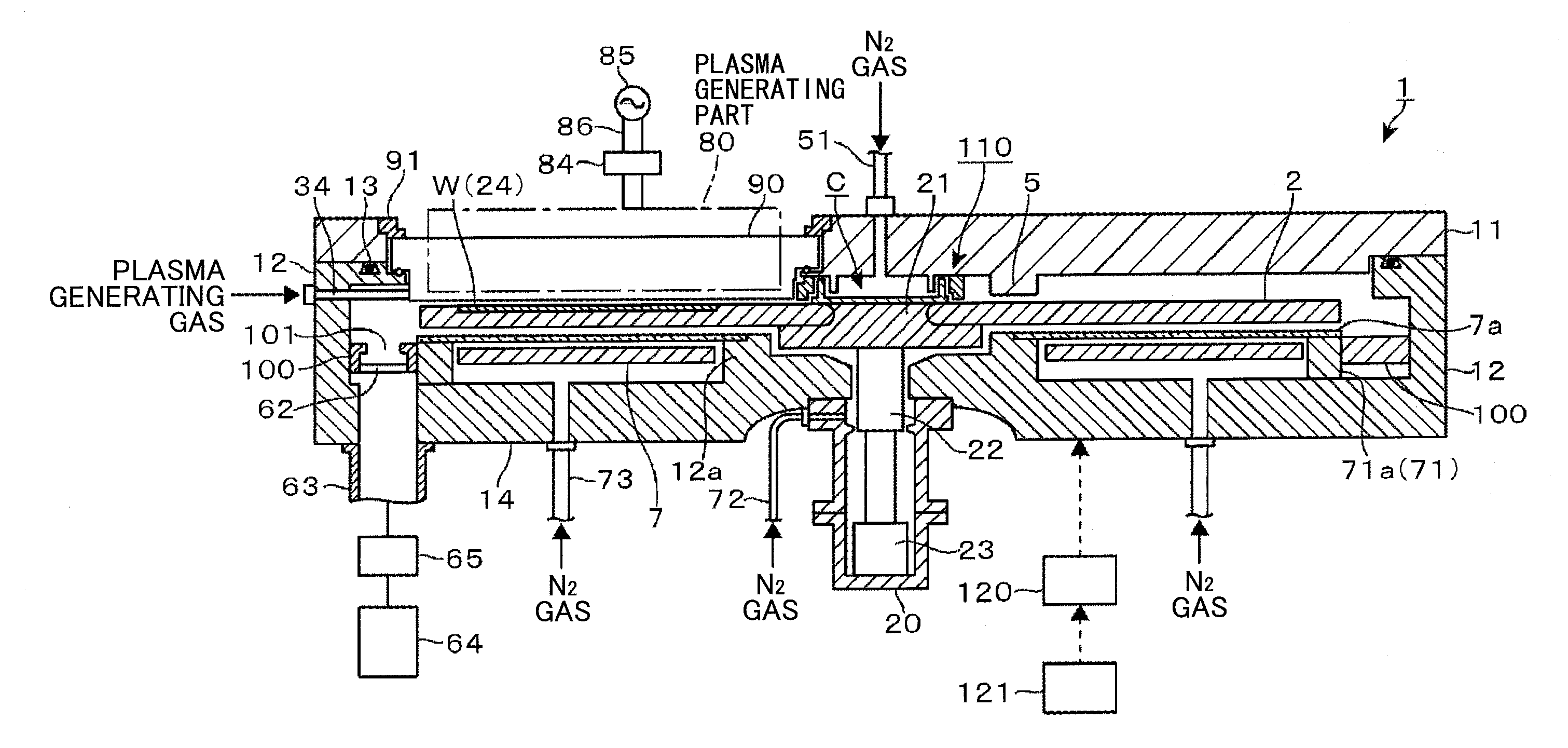
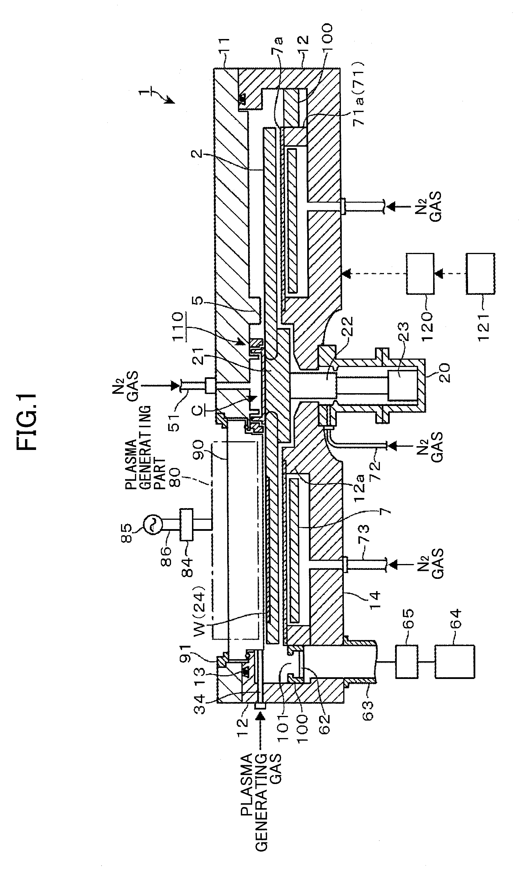
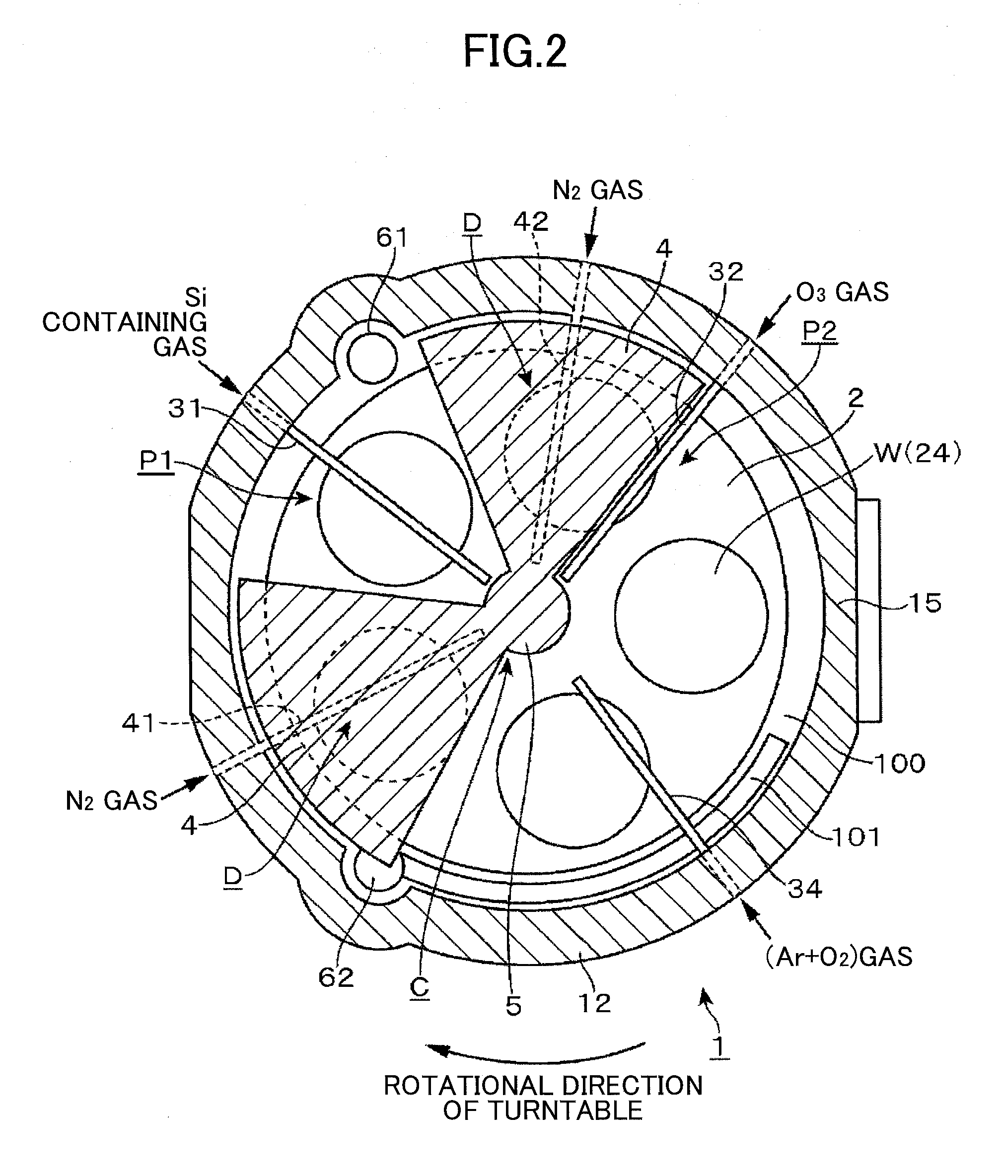
Film deposition apparatus, substrate processing apparatus, and plasma generating device
a substrate processing and plasma generating technology, applied in chemical vapor deposition coatings, electric discharge tubes, coatings, etc., can solve the problems of plasma damage wiring formed inside the wafer, time loss and thereby lowering the wafer throughput, and activated species hardly reaching the wafer, so as to achieve the effect of suppressing plasma damage to the substra
- Summary
- Abstract
- Description
- Claims
- Application Information
AI Technical Summary
Benefits of technology
Problems solved by technology
Method used
Image

Examples
experimental example 1
[0139]Six types of dummy wafers having different permissibility of electrical damage are prepared. Plasma is applied to the wafers via a following Faraday shield. Electric damage to gate oxide films of devices formed on the wafers W is evaluated. Detailed experiment conditions for the embodiment and comparative example are omitted.
Faraday Shield Used for the Experiments
embodiment
[0141]the Faraday shield 95 illustrated in FIG. 8
[0142]When the Faraday shield without the conductive path 97a of the comparative example is experimented, electric damage to wafers occurs as illustrated in the upper half of FIG. 26. In the upper half of FIG. 26, the wafer on the right end has the highest permissibility, and the permissibility of the wafers is lowered in the left direction. On the other hand, when the Faraday shield 95 having the conductive paths 97a, 97a of the embodiment is used, electric damage to the wafers is very small as illustrated in the lower half of FIG. 26. Therefore, it is known that insulation breakdown of the gate oxide film is suppressed by providing the Faraday shield 95 illustrated in FIG. 8.
PUM
| Property | Measurement | Unit |
|---|---|---|
| temperature | aaaaa | aaaaa |
| diameter | aaaaa | aaaaa |
| distance | aaaaa | aaaaa |
Abstract
Description
Claims
Application Information