Multilevel reset voltage for multi-conversion gain image sensor

a multi-level reset and gain image sensor technology, applied in the field of image sensors, can solve the problems of slow image sensor speed, reduced negative effects of charge injection,

Active Publication Date: 2013-02-28
OMNIVISION TECH INC
View PDF2 Cites 28 Cited by
  • Summary
  • Abstract
  • Description
  • Claims
  • Application Information

AI Technical Summary

Problems solved by technology

The detrimental effects of charge injection can also be reduced by reducing clock speeds; however, this leads to a slower speed image sensor.

Method used


Image

  • Multilevel reset voltage for multi-conversion gain image sensor
  • Multilevel reset voltage for multi-conversion gain image sensor
  • Multilevel reset voltage for multi-conversion gain image sensor

Examples


Embodiment Construction

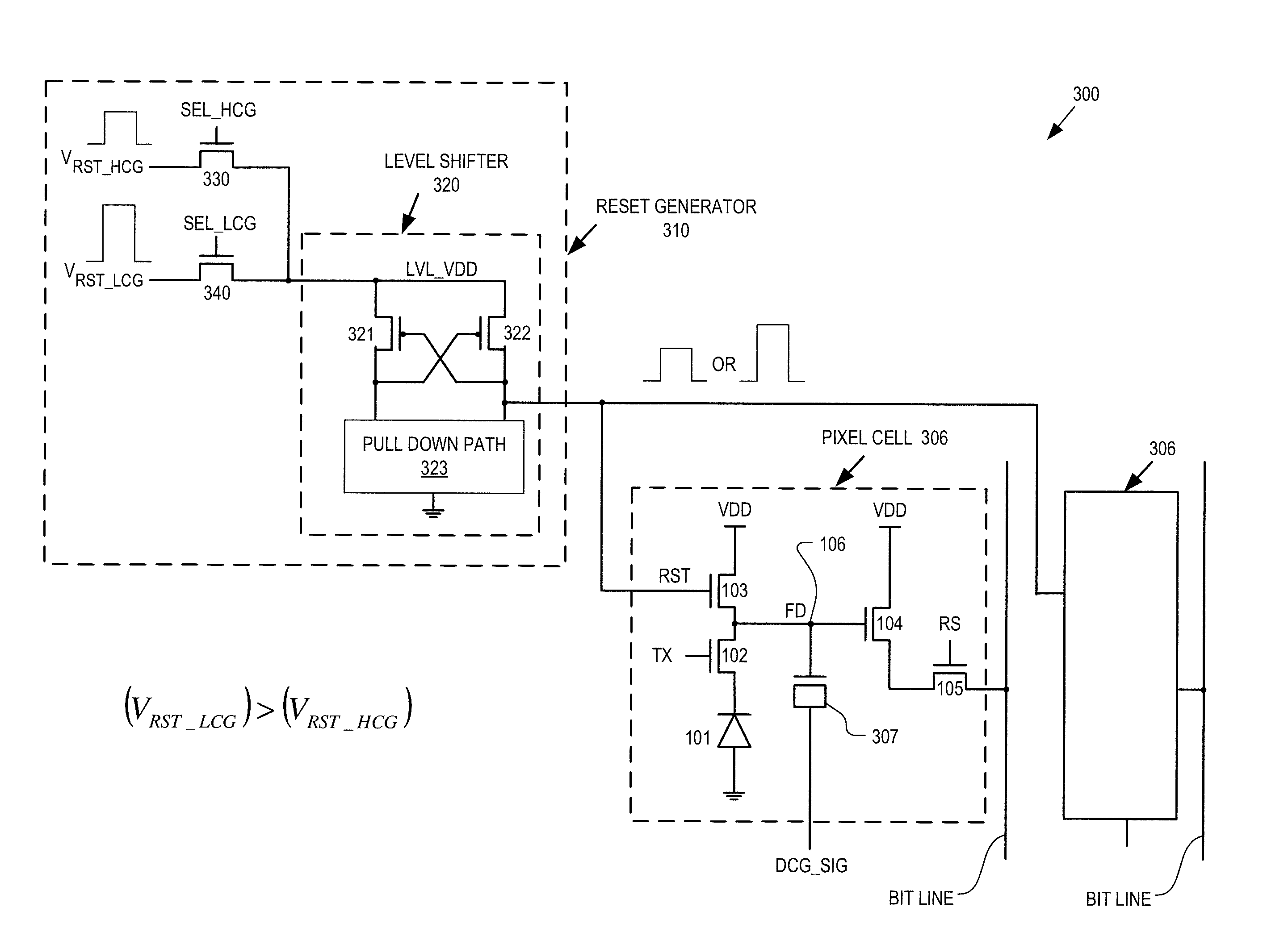
[0018]Embodiments of an apparatus and method of operation for pixel cells having an improved reset gate voltage for dual conversion gain (“DCG”) are described herein. In the following description, numerous specific details are described to provide a thorough understanding of embodiments of the invention. One skilled in the relevant art will recognize, however, that the invention can be practiced without one or more of the specific details or with other methods, components, materials, etc. In other instances, well-known structures, materials or operations are not shown or described but are nonetheless encompassed within the scope of the invention.

[0019]Reference throughout this specification to “one embodiment” or “an embodiment” means that a particular feature, structure, or characteristic described in connection with the embodiment is included in at least one embodiment of the present invention. Thus, the appearances of the phrases “in one embodiment” or “in an embodiment” in vario...


PUM


Abstract

A method of operating an image sensor includes adjusting a capacitance coupled to a circuit node within a pixel cell. The circuit node is coupled to selectively receive an image charge acquired by a photo-sensor of the pixel cell. A conversion gain is selected from multiple conversion gains for the pixel cell by adjusting the capacitance. A voltage level from multiple voltage levels is selected for use as a reset signal when the reset signal is asserted. The reset signal controls resetting of the circuit node during operation of the pixel cell. The voltage level is selected dependent upon which of the multiple conversion gains is selected by adjusting the capacitance. The reset signal is asserted to reset a voltage at the circuit node.

Description

TECHNICAL FIELD[0001]This disclosure relates generally to image sensors, and in particular, but not exclusively to complementary metal-oxide semiconductor (“CMOS”) image sensors.BACKGROUND INFORMATION[0002]Image sensors have become ubiquitous. They are widely used in digital still cameras, cellular phones, security cameras, as well as, medical, automobile and other applications. The technology used to manufacture image sensors, and in particular complementary metal-oxide-semiconductor (“CMOS”) image sensor, has continued to advance at great pace. For example, the demands of higher resolution and lower power consumption have encouraged the further miniaturization and integration of these image sensors.[0003]FIG. 1A is a circuit diagram illustrating pixel circuitry of a four-transistor (“4T”) pixel cell 100 within an image sensor array. Pixel cell 100 may be repeated and organized into rows and columns of the image sensor array. Pixel cell 100 includes a photodiode 101, a transfer tra...

Claims


Application Information

Patent Timeline
Patent Type & Authority Applications(United States)
IPC IPC(8): H01L27/146
CPCH04N5/3598H04N5/3559H04N25/59H04N25/627
Inventor BIKUMANDLA, MANOJ
Owner OMNIVISION TECH INC
Why Eureka
Try Eureka