Switching circuit and envelope signal amplifier

Inactive Publication Date: 2013-02-28
TOYOHASHI UNIVERSITY OF TECHNOLOGY +1
View PDF4 Cites 0 Cited by
  • Summary
  • Abstract
  • Description
  • Claims
  • Application Information

AI Technical Summary

Benefits of technology

[0020]According to the switching circuit described above, the switching elements are sequentially switched at a constant time interval by the PWM signal propagating through the connection circuit, and the PWM signals of substantially equal amplitude that are amplified at the switching elements are added up at the other end of the second inductance element.
[0021]When the abovementioned switching circuit receives input of a PWM signal that has a modulation cycle equivalent to N times the abovementioned time interval, signal points corresponding to the amplitudes and phases of the PWM signals output to the one ends of the switching elements based on the fundamental waves of the PWM signal are arranged on a circle around the origin in a complex plane, at a regular interval with a phase difference

Problems solved by technology

However, it is technically difficult for the class D amplifier to enhance the withstand voltages of the complementary switching elements in a balanced manner.
For th

Method used


Image

  • Switching circuit and envelope signal amplifier
  • Switching circuit and envelope signal amplifier
  • Switching circuit and envelope signal amplifier

Examples


embodiment 2

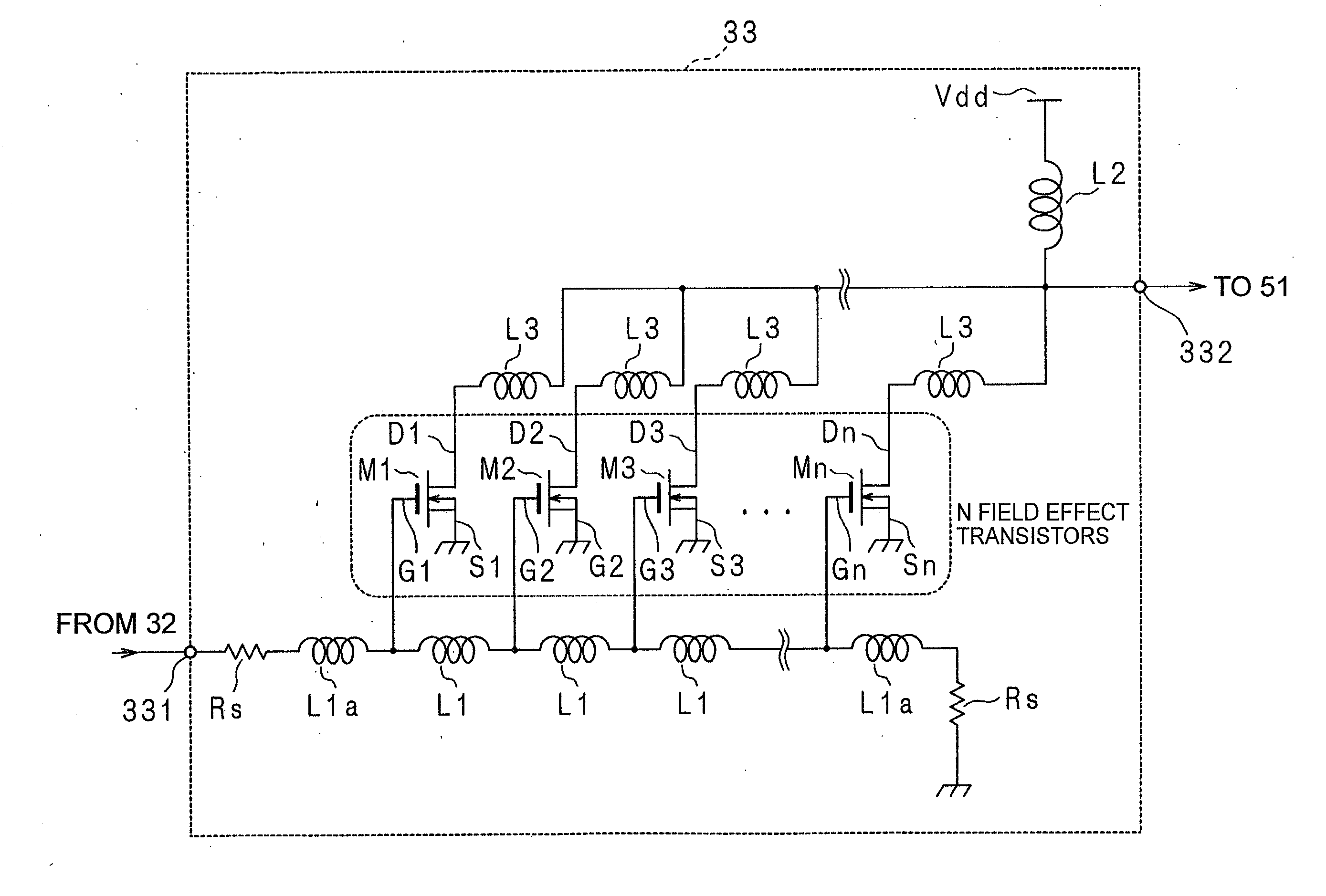
[0063]Embodiment 1 does not exclude an option of configuring the switching circuit 33 with discrete parts on a circuit board. In Embodiment 2, on the other hand, a switching circuit is formed on a semiconductor substrate, as an IC.

[0064]FIG. 6 is a schematic plan view of a switching circuit 33a according to another embodiment (Embodiment 2). The switching circuit 33a is formed on a semiconductor substrate of a monolithic integrated circuit. The switching circuit 33a has the coil L2 having one end connected to the power supply Vdd, and sixteen transistors M1 to M16. The other end of the coil L2 is connected to drains D1 to D16 by conductor patterns (connecting members). Sources S1 to S16 of the respective transistors M1 to M16 are connected to a ground potential (the ground potential is partially marked with diagonal lines in FIG. 6). The other end of the coil L2 is configured as the output terminal 332 of the switching circuit 33a.

[0065]Gates G1 to G16 of the respective transistors...

embodiment 3

[0072]In Embodiment 2 the vertical MOSFETs are provided on a semiconductor substrate. In Embodiment 3, on the other hand, high-withstand voltage / high-power vertical MOSFETs are provided on the same semiconductor substrate.

[0073]FIG. 7 is a schematic plan view of a switching circuit 33b according to yet another embodiment (Embodiment 3). In (A) and (B) of FIG. 7, plan views illustrating front and rear surfaces of the switching circuit 33b are shown, respectively. The switching circuit 33b is formed on a semiconductor substrate of a monolithic integrated circuit and has transistors M1, M2, . . . , M8 of vertical MOSFETs that are disposed in a circular pattern. Sources S1 to S8 and gates G1 to G8 of the transistors M1, M2, . . . , M8 are formed on the front surface of the semiconductor substrate, whereas drains D1, D2, . . . , D8 of the respective transistors M1, M2, . . . , M8 are formed on the rear surface of the semiconductor substrate.

[0074]Sources S1 to S16 of transistors M1 to M1...


PUM


Abstract

A switching circuit according to one embodiment has: N switching elements; a connection circuit including N−1 first inductance elements that are connected in series; a second inductance element; and N third inductance elements. Control terminals of the N switching elements are connected to ends of the connection circuit and connection contacts, respectively. One end of the second inductance element is connected to a power supply. The N third inductance elements electrically connects one ends of the N switching elements and the other end of the second inductance element with each other, respectively.

Description

TECHNICAL FIELD[0001]The present invention relates to a switching circuit for switching a switching element, which is connected to an inductance element, with a PWM (Pulse Width Modulation) signal. The present invention also relates to an envelope signal amplifier including the switching circuit.BACKGROUND ART[0002]In recent years, an EER (Envelope Elimination and Restoration) system has been used as one of the amplification systems used for power-amplifying a high-frequency modulation signal in a base station of a cellular phone, etc. The EER system amplifies a signal by extracting an amplitude component (envelope) and phase component from a modulation signal to be amplified, and modulating the amplitude of a signal corresponding to the phase component with a signal corresponding to the amplitude component, so that the amplitude of the modulated signal becomes proportional to the amplitude of the original modulation signal.[0003]More specifically, voltage that follows the extracted...

Claims


Application Information

Patent Timeline
IPC IPC(8): H03F3/217H01H47/00
CPCH01L23/645H01L23/66H01L2924/13091H01L2223/6644H03F1/18H03F3/217H03F2200/102H03F2200/351H03F1/0227H03F3/2176H03F3/2178H03F3/607H02M2003/1586H03F2200/366H01L2224/48227H01L2924/00H02M3/1586H03F1/02
Inventor OHIRA, TAKASHIWADA, KAZUYUKINAKATA, MITSUTOSHISAWADA, KAZUSHIHATSUKAWA, SATOSHISHIGA, NOBUOFUJIKAWA, KAZUHIRO
Owner TOYOHASHI UNIVERSITY OF TECHNOLOGY
Why Eureka
Try Eureka