Via structure for transmitting differential signals

Active Publication Date: 2013-03-07
SAMTEC
View PDF4 Cites 33 Cited by
  • Summary
  • Abstract
  • Description
  • Claims
  • Application Information

AI Technical Summary

Benefits of technology

[0013]To overcome the problems described above, preferred embodiments of the present invention provide a via structure that can be used in high-density, high-speed connector applications that require high-performance PCB breakout designs to enable full utilizatio

Problems solved by technology

The prior art via structures described above fail to include a single central axis of signal propagation through the transition from the connector to the PCB.
Further, the prior art via structures lack angular symmetry with respect to the top ground plane layer and lack preferential coupling between the vias of the differential signals because the cross term coupling factors are evenly distributed.
The failure to include a single central axis of signal propagat

Method used


Image

  • Via structure for transmitting differential signals
  • Via structure for transmitting differential signals
  • Via structure for transmitting differential signals

Examples


Example

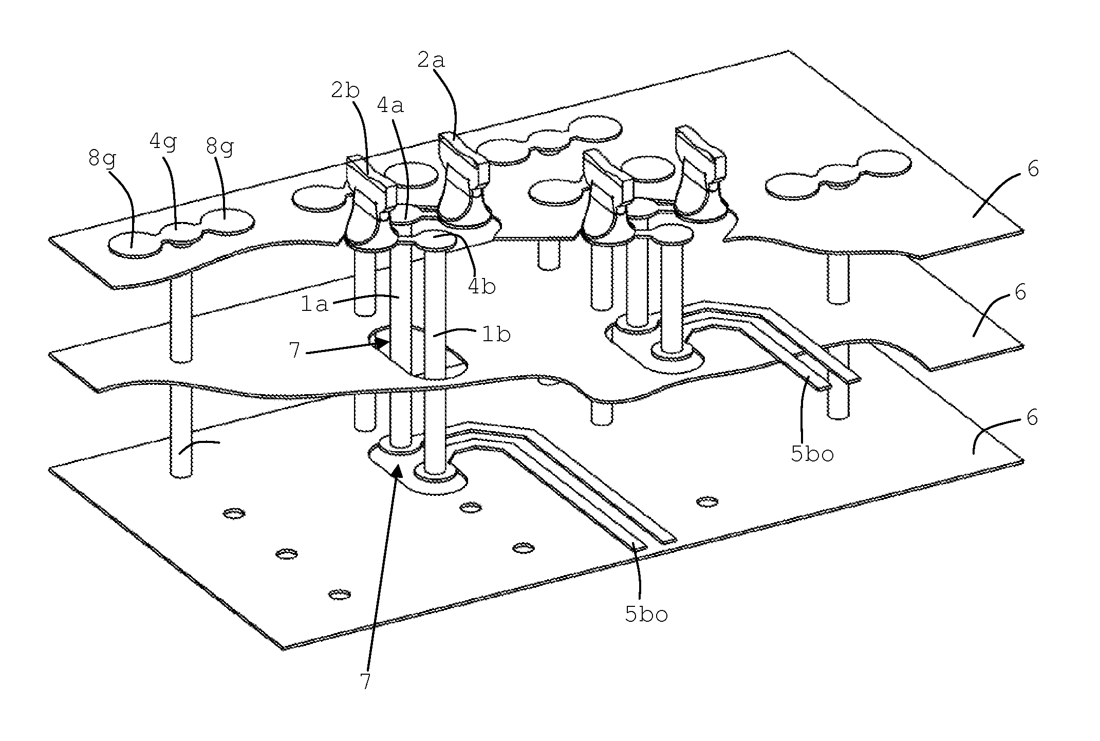
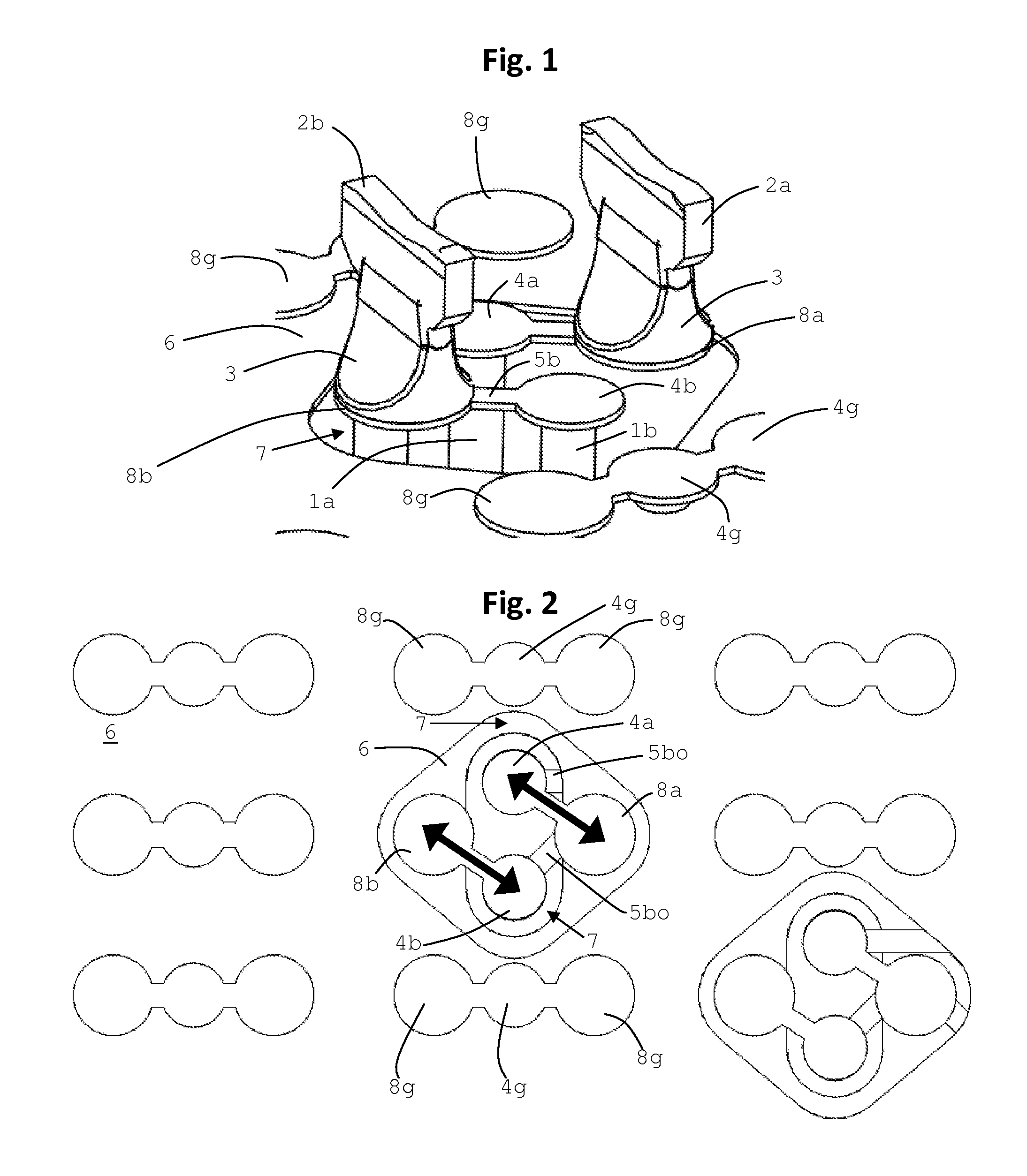
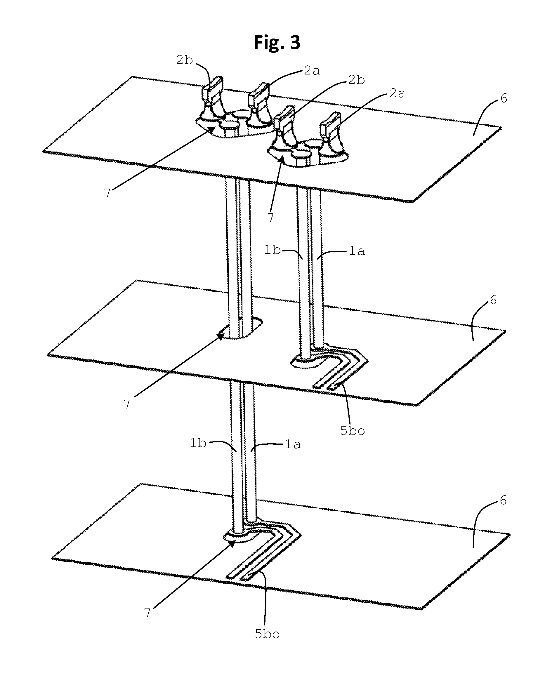
[0051]FIGS. 1-15 and 23A-25 show preferred embodiments of the present invention. FIGS. 1-15 show via structures according to various preferred embodiments of the present invention. FIGS. 23A-25 show a connector connected to via structure according to a preferred embodiment of the present invention.

[0052]FIG. 1 is a close-up view of contacts 2a, 2b that are arranged as a differential pair. FIG. 2 is a plan view of a six-by-three array of pads 8, in which contacts 8a, 8b are surrounded by contacts 8g. In FIGS. 1 and 2, as well as some of the other figures, certain elements or features are left-out for illustrative purposes. For example, only the conductive portions of the PCB are shown in FIGS. 1 and 2, while the dielectric portions (e.g., layers of FR-4 or other suitable dielectric materials) are not shown. In addition, some the elements or features are exaggerated in some of the figures. For example, the distance between the ground planes 6 in FIG. 3 is exaggerated so that BOR can b...


PUM


Abstract

A printed circuit board including first and second signal pads located on a top surface of the printed circuit board and arranged to transmit a first differential signal, first and second signal vias extending through the printed circuit board and arranged to transmit the first differential signal, and a first ground plane located on a layer below the top surface of the printed circuit board and including an antipad that encompasses the first and second signal pads and the first and second signal vias when viewed in plan.

Description

[0001]U.S. Applications Nos. (Attorney Docket No. 80505.125) and (Attorney Docket No. 80505.133) filed on Sep. 7, 2012 are directed to similar subject matter as this application and are incorporated by reference in their entireties.BACKGROUND OF THE INVENTION[0002]1. Field of the Invention[0003]The present invention relates to a via structure of a printed circuit board (PCB). More specifically, the present invention relates to the via structure of a PCB for transmitting differential signals.[0004]2. Description of the Related Art[0005]It is known to use differential signaling to transmit information. Differential signaling uses two complementary signals that are sent on two paired transmission lines, e.g. contacts, wires, or traces. These paired transmission lines are referred to as differential pairs, and the complementary signals are referred to as differential signals. The differential signals are typically transmitted through a connector and a PCB. In the connector, the differen...

Claims


Application Information

Patent Timeline
IPC IPC(8): H05K1/11
CPCH05K1/0245H05K3/4015H05K1/0251
Inventor BIDDLE, GARY ELLSWORTHNADOLNY, JAMES
Owner SAMTEC
Why Eureka
Try Eureka