Plate

Active Publication Date: 2013-03-07
GENESIS PHOTONICS
View PDF5 Cites 25 Cited by
  • Summary
  • Abstract
  • Description
  • Claims
  • Application Information

AI Technical Summary

Benefits of technology

[0007]The present invention provides a plate, which can overcome the problem that

Problems solved by technology

When the LED chip is packaged by the above eutectic technique, the metal reflection layer of the plate may be exposed to a

Method used


Image

  • Plate
  • Plate
  • Plate

Examples


first embodiment

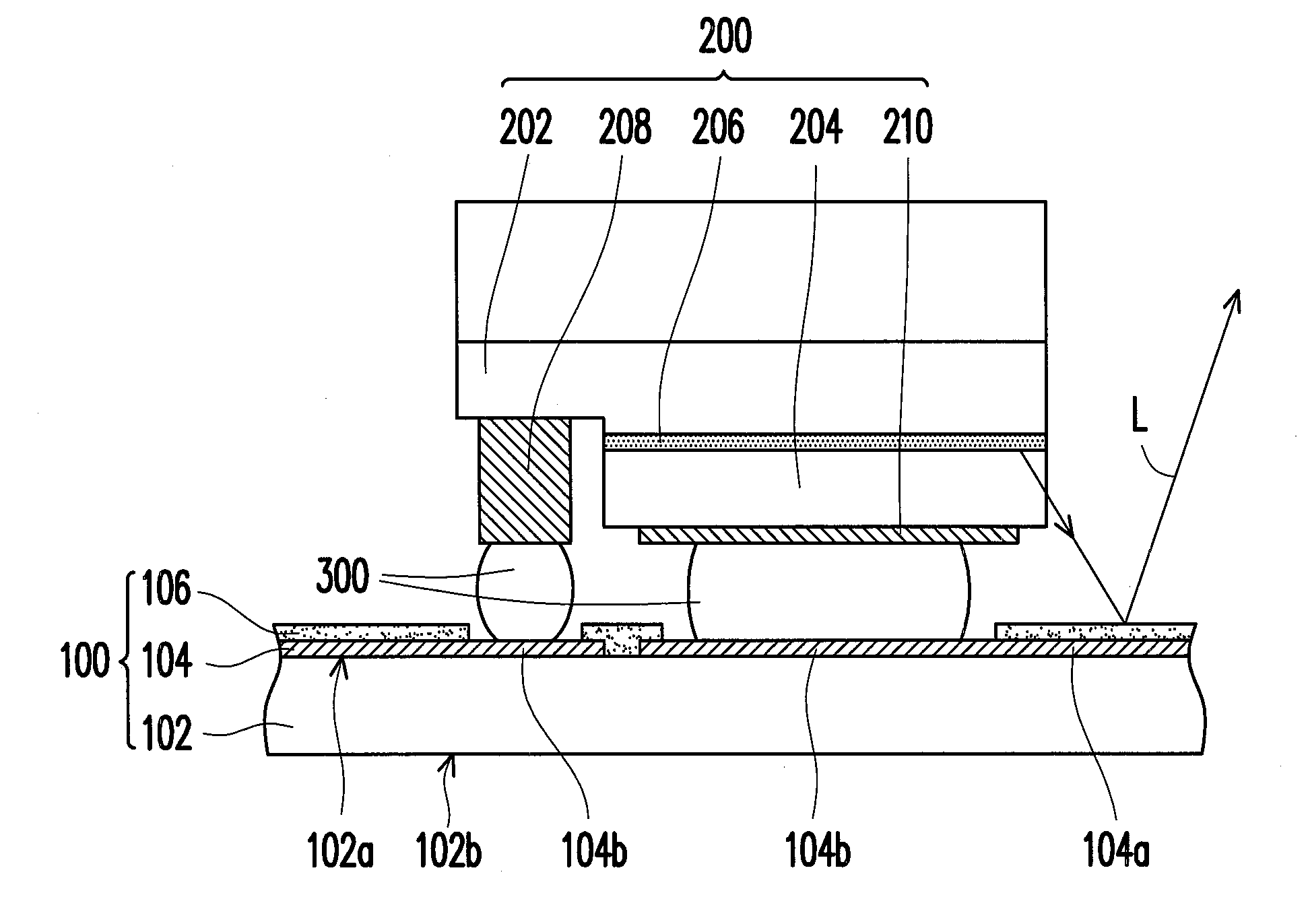
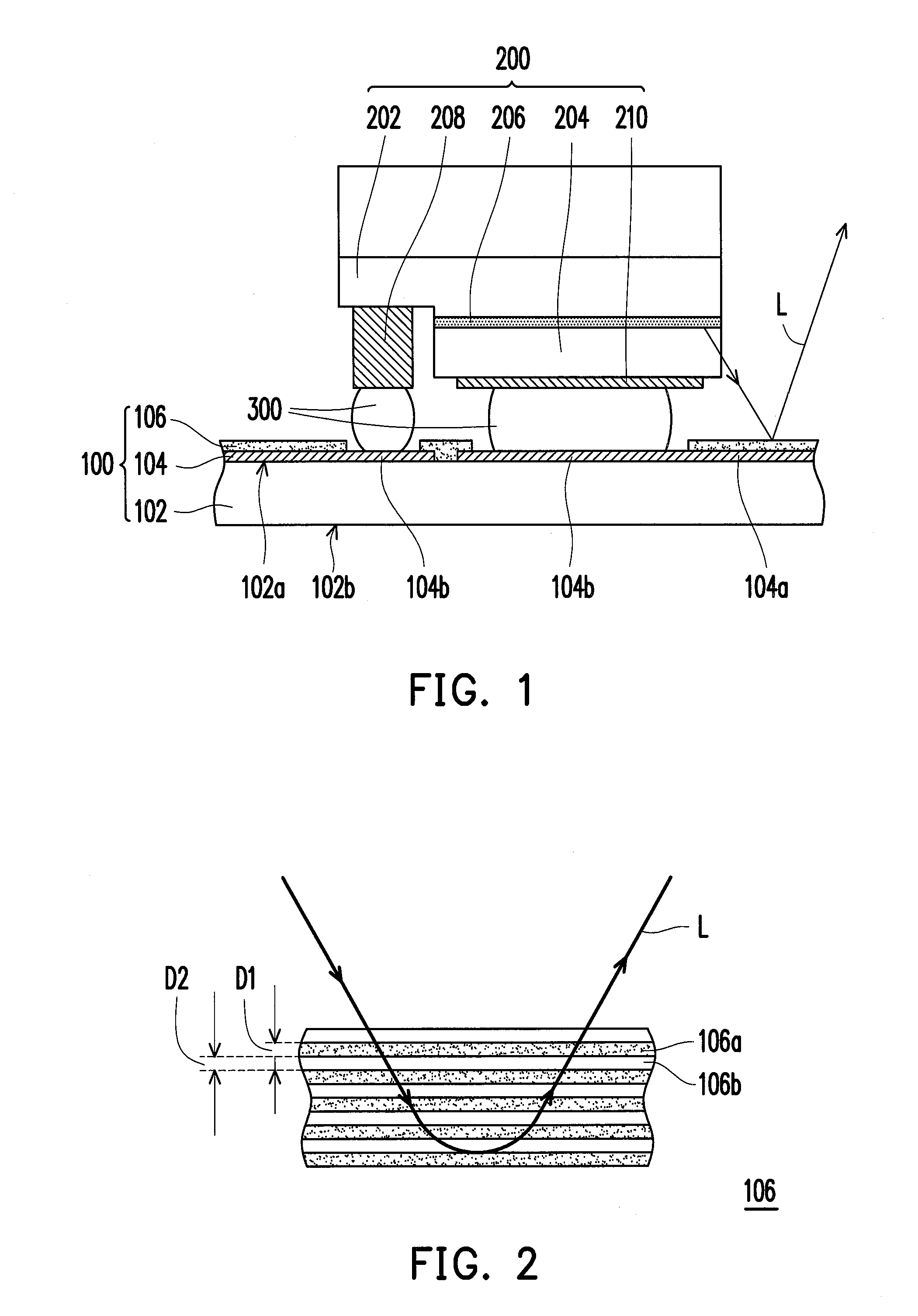
[0029]FIG. 1 is a schematic cross-sectional view of a plate according to a first embodiment of the present invention. Referring to FIG. 1, at least one flip-chip LED chip 200 is adapted to be disposed on a plate 100 of this embodiment. In FIG. 1, one flip-chip LED chip 200 is illustrated for example; however, the number of the flip-chip LED chips that can be carried on the plate of the present invention is not particularly limited. In other words, the plate 100 of the present invention may carry a plurality of flip-chip LED chips 200. In this embodiment, the flip-chip LED chip 200 includes a first-type doped semiconductor layer 202, a second-type doped semiconductor layer 204, a light-emitting layer 206, a first electrode 208 and a second electrode 210. The light-emitting layer 206 is disposed between the first-type doped semiconductor layer 202 and the second-type doped semiconductor layer 204. The first electrode 208 and the second electrode 210 respectively are disposed on the fi...

second embodiment

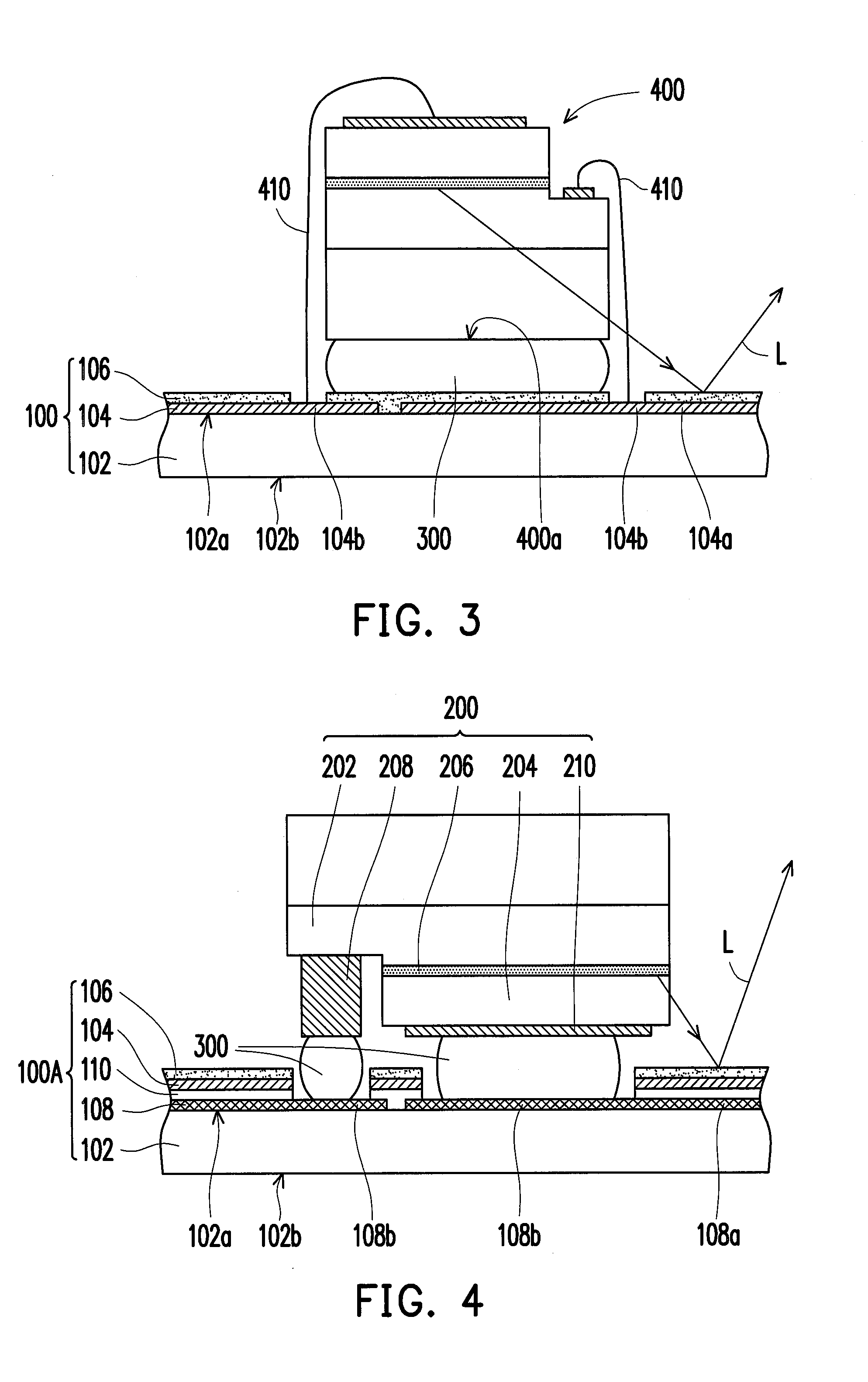
[0037]FIG. 4 is a schematic cross-sectional view of a plate according to a second embodiment of the present invention. Referring to FIG. 4, the plate 100A of this embodiment is similar to the plate 100 of the first embodiment. Therefore, the same parts are indicated by the same symbols in FIG. 1. The difference between the two lies in that the wiring structure and the bonding pads of this embodiment are not fabricated in the metal reflection layer 104, but are fabricated in the conductive layer 108 between the first surface 102a and the metal reflection layer 104. Hereinafter, only the difference is illustrated and the details of the same parts will not be repeated herein.

[0038]Referring to FIG. 4, at least one flip-chip LED chip 200 is adapted to be disposed on the plate 100A of this embodiment. The plate 100A of this embodiment includes a substrate 102, a metal reflection layer 104 and an oxidation protection layer 106. The substrate 102 has a first surface 102a and a second surfa...


PUM


Abstract

A plate including a substrate, a metal reflection layer and an oxidation protection layer is provided. The substrate has a first surface and a second surface opposite to the first surface. The metal reflection layer is disposed on the first surface of the substrate. The oxidation protection layer covers the metal reflection layer. The metal reflection layer is disposed between the oxidation protection layer and the first surface of the substrate. At least one light emitting diode chip is adapted to eutectic bonding on the plate.

Description

CROSS-REFERENCE TO RELATED APPLICATION[0001]This application claims the priority benefit of Taiwan application serial no. 100132134, filed on Sep. 6, 2011. The entirety of the above-mentioned patent application is hereby incorporated by reference herein and made a part of this specification.BACKGROUND OF THE INVENTION[0002]1. Field of the Invention[0003]The present invention relates to a plate, and more particularly to a plate adapted to eutectic bonding a light emitting diode (LED) chip.[0004]2. Description of Related Art[0005]As the environment protection consciousness rises nowadays, in addition to desperately searching a renewable energy source, people also put efforts on development of power saving products. For an illumination product, a power saving and environmental friendly light source, that is an LED chip, has been developed. The LED chip generates light by recombination of electrons and holes on a P-N junction. Compared with the conventional light sources, the LED chip h...

Claims


Application Information

Patent Timeline
IPC IPC(8): H01L33/60
CPCH01L2224/73265H01L33/60H05K2201/10106H05K2201/2054H01L2224/48227H01L2224/48228H01L2224/1403H01L2933/0066H01L2224/48091H01L2224/16225H01L2924/01322H05K3/3431H01L2224/32225H01L33/62H01L2224/49107H01L2924/00014H01L2924/00012H01L2924/00H01L24/73
Inventor SU, PO-JENLI, YUN-LI
Owner GENESIS PHOTONICS
Why Eureka
Try Eureka