

Liquid crystal display device
a liquid crystal display and display device technology, applied in non-linear optics, instruments, optics, etc., can solve problems such as image quality degradation, achieve the effects of increasing the production yield of liquid crystal display devices, and preventing the scraping of oriented films
- Summary
- Abstract
- Description
- Claims
- Application Information
AI Technical Summary
Benefits of technology
Problems solved by technology
Method used
Image

Examples
first embodiment
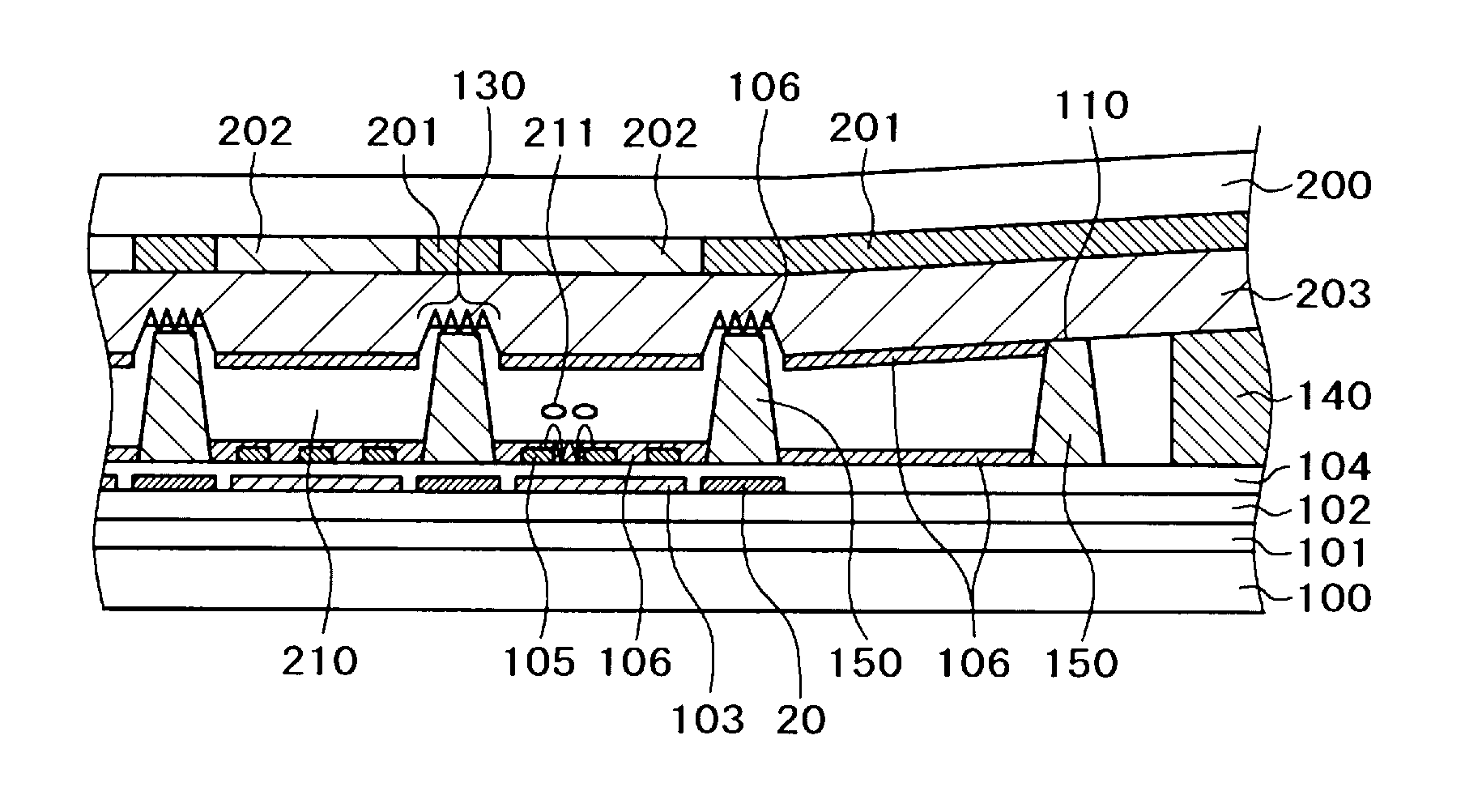
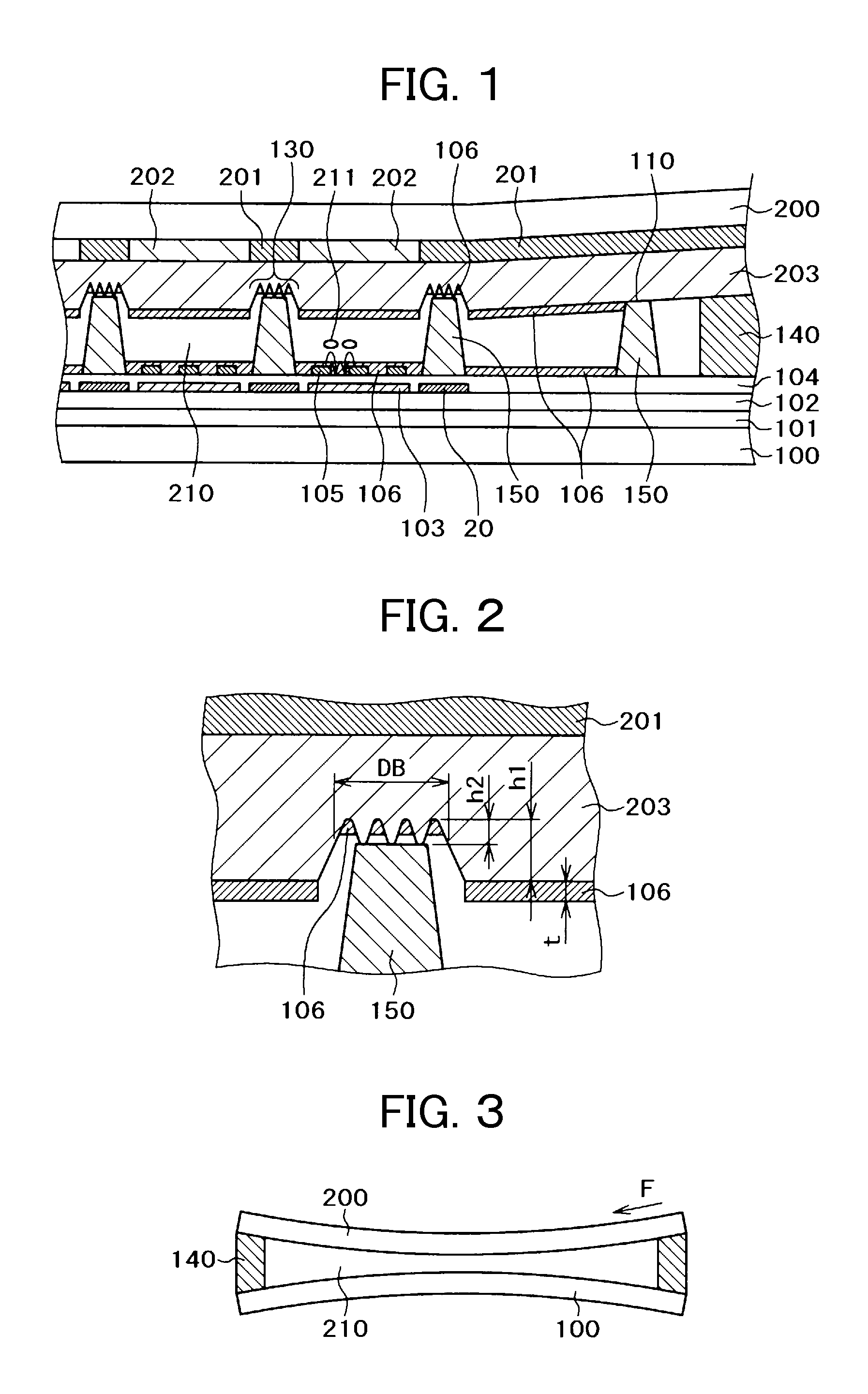
[0040]FIG. 1 is a cross-sectional view, showing the present invention in an end portion of a liquid crystal display device. FIG. 1 is a cross-sectional view of an IPS mode liquid crystal display device in which the organic passivation film 107 is not used. In FIG. 1, the area in which color filters 202 are formed in the counter substrate 200 is the display area. Then, the area close to the sealing material 140 is the peripheral area. In FIG. 1, a gate insulating film 101 is formed on the TFT substrate 100. Then, a passivation film 102 is formed on the gate insulating film 101. The passivation film 102 protects TFT not shown.
[0041]A pixel electrode 103 is formed flat for each pixel on the passivation film 102. Further, image signal lines 20 are also formed on the passivation film 102. An interlayer insulting film 104 is formed to cover the pixel electrode 103 and the image signal lines 20. A comb-like counter electrode 105 is formed on the pixel electrode 103 with the interlayer insu...
second embodiment
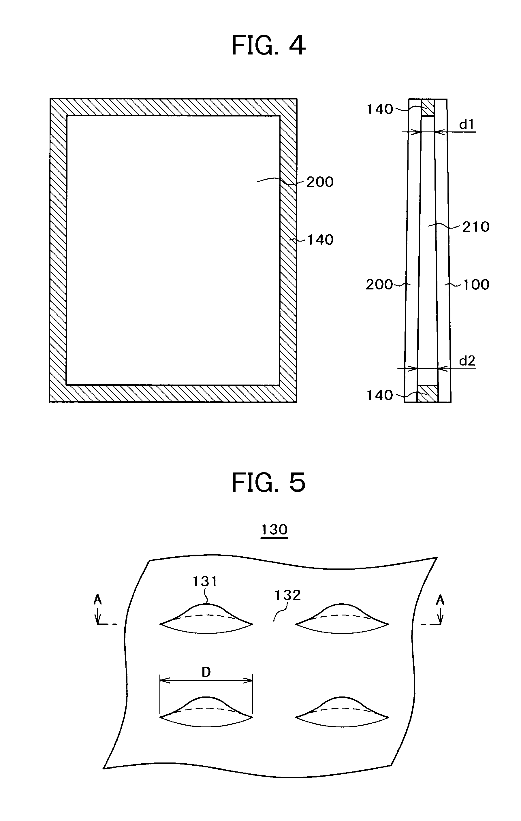
[0060]FIG. 11 is a perspective view showing the shape of the bottom surface of the concavo-convex mount 130 according to a second embodiment of the present invention. The concavo-convex mount 130 is formed in the overcoat film 203 of the counter substrate 200. In FIG. 11, the concave-convex pattern of the bottom surface of the concavo-convex mount 130 is formed only in one direction (x-direction). In other words, in FIG. 11, the concave-convex pattern is sequentially formed in the horizontal direction (x-direction) at a predetermined pitch P, and the ridge of the concave portion 131 is formed in the vertical direction (y-direction). Also in the shape of FIG. 11, the oriented film 106 is not present in the convex portion 131. The oriented film 106 is made thick in the concave portion 132.
[0061]In FIG. 11, the cylindrical spacer 150 is brought into contact with the convex portion 131. However, the oriented film 106 is not present in the convex portion 131. Thus, the oriented film 106 ...
PUM
| Property | Measurement | Unit |
|---|---|---|
| tilt angle | aaaaa | aaaaa |
| tilt angle | aaaaa | aaaaa |
| tilt angle | aaaaa | aaaaa |
Abstract
Description
Claims
Application Information