Light emitting device

Inactive Publication Date: 2013-03-28
KIJIMA NAOTO +4
View PDF13 Cites 18 Cited by
  • Summary
  • Abstract
  • Description
  • Claims
  • Application Information

AI Technical Summary

Benefits of technology

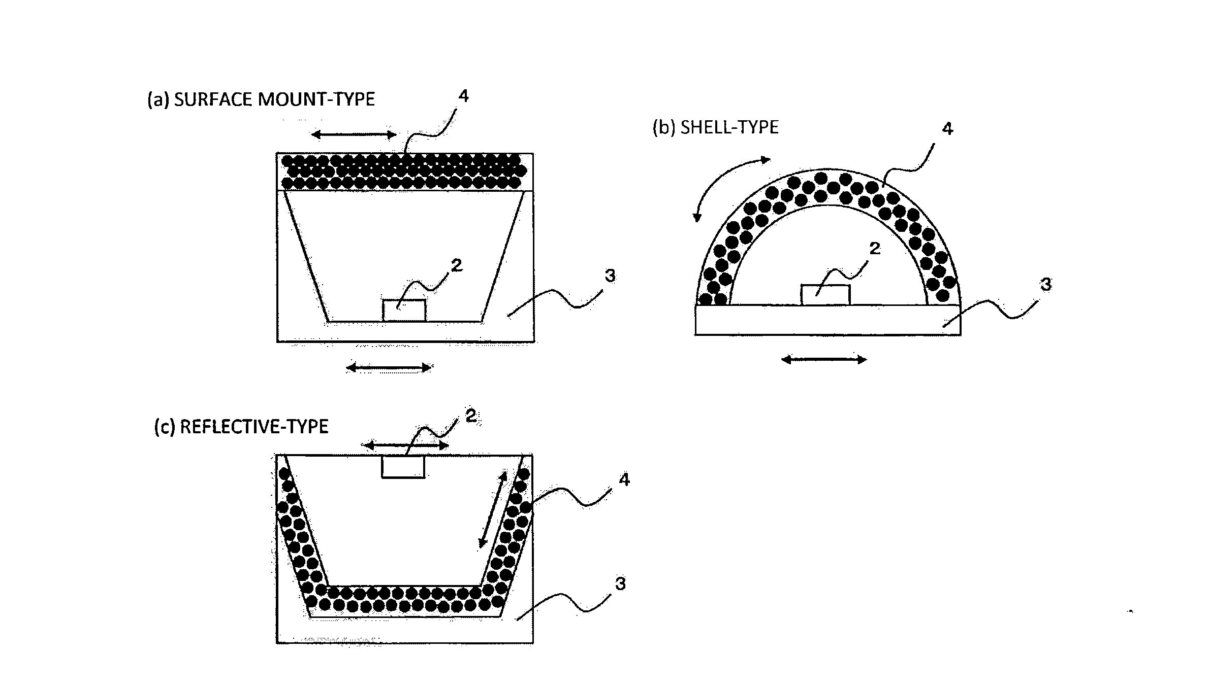
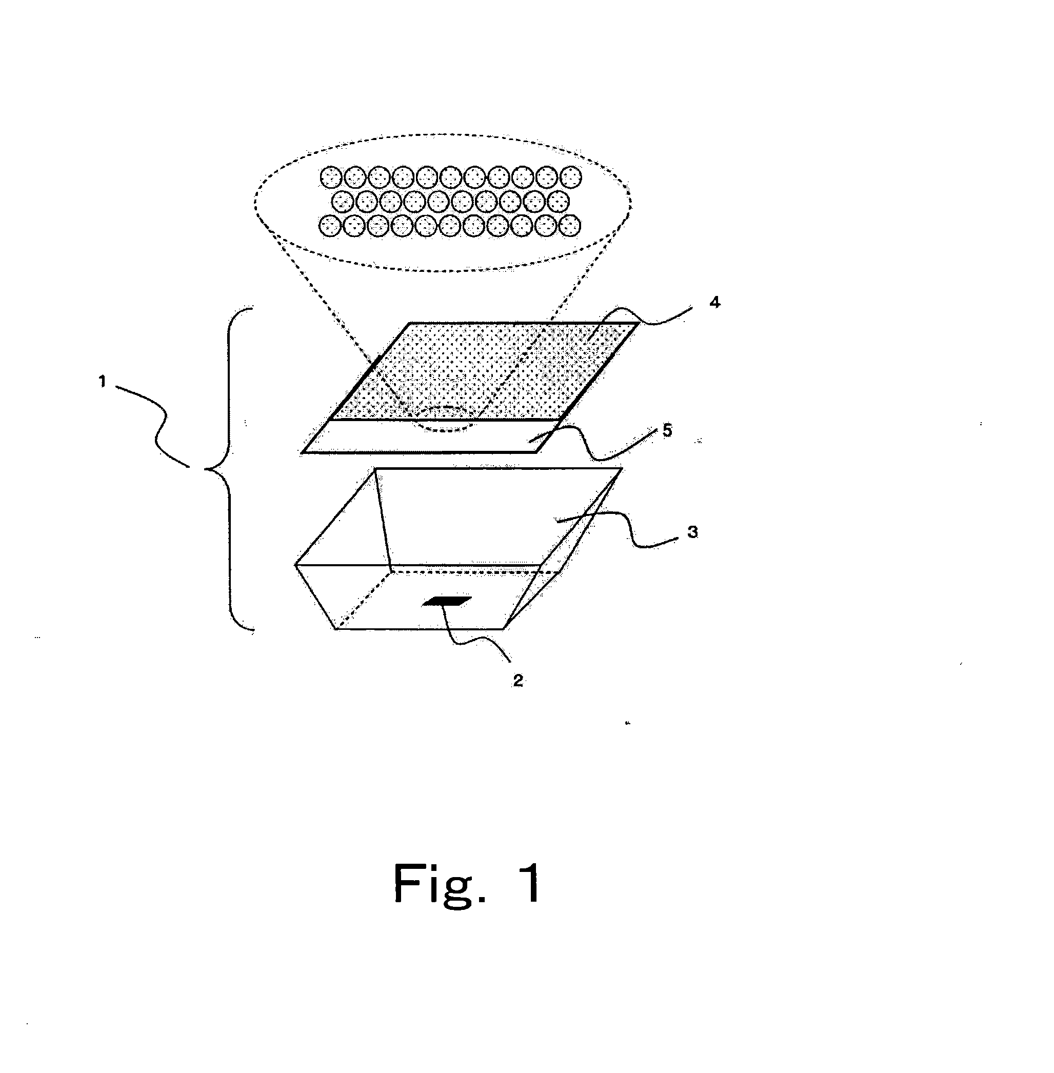
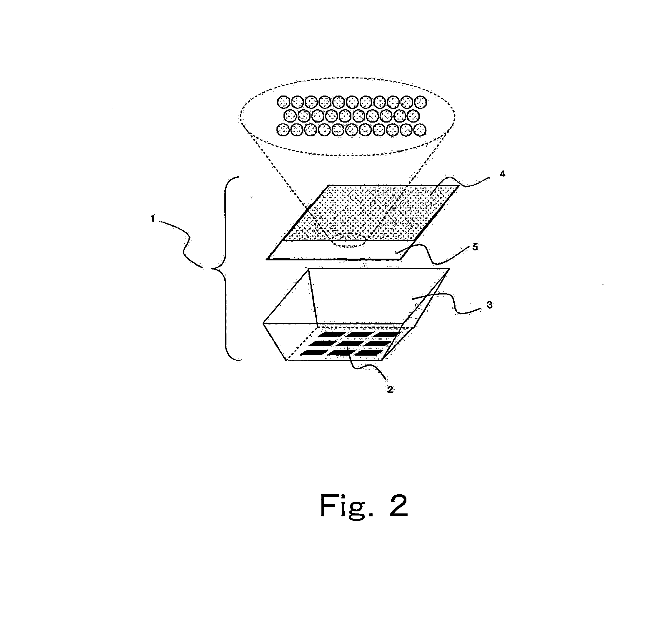
The present invention is a light emitting device that improves the emission efficiency of the phosphor layer by reducing self-absorption and the absorption of light by the resin, and prevents light scattering caused by the phosphor to increase the efficiency of light extraction. This is achieved by using a thin and delicate phosphor layer with specific values for its thickness and packing ratio.

Problems solved by technology

However, the light emitting element according to Patent Document 1 is confronted by the problem that, in using a phosphor layer of a large thickness, in the fluorescent light emitted from the phosphor which is disposed in a position close to the semiconductor light emitting element also in the phosphor layer, there is a large proportion of light which is self-absorbed by phosphor of the same type until the emission surface is reached or there is a large proportion of light which is absorbed by the encapsulating resin until the emission surface is reached and, as a result, the emission efficiency of the phosphor layer is low (first problem).
The light emitting element according to Patent Document 1 is confronted by the problem that, in using a phosphor layer of a large thickness, in the fluorescent light emitted from the phosphor which is disposed in a position close to the semiconductor light emitting element also in the phosphor layer, there is a large proportion of light which is scattered by other phosphor until the emission surface is reached and, as a result, light extraction efficiency of the phosphor layer is low (second problem).
Further, if the phosphor layer comprises a mixture of a plurality of phosphors of different emission colors, a phenomenon arises whereby phosphor of another type absorbs the fluorescent light emitted by a certain type of phosphor and so-called cascade excitation arises, and the light emission efficiency of the phosphor layer is low (third problem).
In addition, as per the light emitting device according to Patent Document 1, if the phosphor layer is configured to directly cover the semiconductor light emitting element, as the light output of the semiconductor light emitting element increases, not only does the temperature of the semiconductor light emitting element rise, but also the temperature of the phosphor rises due to the heat generated through loss at the time of color conversion of the phosphor and, as a result, the emission efficiency of the semiconductor light emitting element and the phosphor layer is low (fourth problem).

Method used


Image

  • Light emitting device
  • Light emitting device
  • Light emitting device

Examples


example 1

[0189]The value of the total luminous flux in a case where the volume packing ratio of the phosphor in the phosphor layer was changed in the light emitting device shown in FIG. 11 was studied via simulation.

[0190]More specifically, a light emitting device was fabricated in which a blue-color LED with an emission peak wavelength of 450 nm was used as the semiconductor light emitting element and a phosphor layer obtained by maintaining uniform dispersion of phosphor in the binder resin was used as the phosphor layer, and in which the semiconductor light emitting element and the phosphor layer were disposed spaced apart at a distance of 0.5 mm. As the phosphor contained in the phosphor layer, a CSMS phosphor with a peak wavelength of 514 nm which is represented as Ca3 (Sc, Mg)2Si3O12:Ce (volume median diameter: 12 μm) and a SCASN phosphor with a peak wavelength of 630 nm which is represented as (Sr, Ca) AlSiN3:Eu (volume median diameter: 10 μm) were used and, as the binder resin which ...

example 2

[0193]A light emitting device which comprises a semiconductor light emitting element module and a phosphor layer was fabricated and the total luminous flux was measured.

[0194]As the semiconductor light emitting element module, a single 350 μm square InGaN LED chip with a principal emission peak wavelength of 405 nm which is formed using a sapphire substrate was stuck to the cavity bottom face of a 3528 SMD-type PPA resin package by using a transparent diebond paste with a silicone resin base. Following adhesion and after hardening the diebond paste by applying heat for two hours at 150°, an LED chip side electrode and a package side electrode were connected using Au wire with a diameter of 25 μm. Two bonding wires were employed.

[0195]The phosphor mix ratio is suitably adjusted such that the content of the phosphor in the phosphor layer is a volume packing ratio of 35% and such that the correlated color temperature of the light emitted by the light emitting device is approximately 58...

example 3

[0199]Other than the fact that the content of the phosphor in the phosphor layer is a volume packing ratio of 21%, a light emitting device was fabricated similarly to that of Example 2 and comprising a semiconductor light emitting module and a phosphor layer and the emission spectrum was measured.

[0200]The values of various light emission characteristics (chromaticity coordinates (Cx, Cy), correlated color temperature, total luminous flux) which were calculated from the emission spectrum obtained are shown in Table 1.


PUM


Abstract

An object of the present invention is to provide a light emitting device which increases the emission efficiency of phosphor by reducing self-absorption of light by phosphor and by reducing absorption of fluorescent light by an encapsulating resin, and which increases the efficiency of light extraction from the phosphor layer by preventing light scattering caused by the phosphor.The above object was achieved by a light emitting device comprising a semiconductor light emitting element and a phosphor layer wherein the phosphor layer was made dense by setting specific values for particle distribution of phosphor contained in the phosphor layer and for the packing ratio of the phosphor contained in the phosphor layer.

Description

TECHNICAL FIELD[0001]The present invention relates to a light emitting device and, more particularly, to a light emitting device exhibiting high emission efficiency and including a phosphor layer of a high light extraction efficiency.BACKGROUND ART[0002]A light emitting device which uses a semiconductor light emitting element holds a phosphor in an encapsulating resin which covers the light emitting element and color-converts, by means of the phosphor, the light which is irradiated from the light emitting element before irradiating the light to the outside. For example, Patent Document 1 discloses a light emitting device which comprises a phosphor layer containing a phosphor and an encapsulating resin and with which breakage of bonding wires electrically connecting the semiconductor light emitting element can be prevented by setting specific values for the film thickness of the phosphor layer and for the volume packing ratio of the phosphor contained in the phosphor layer.[0003]Japa...

Claims


Application Information

Patent Timeline
IPC IPC(8): H01L33/50
CPCH01L33/502H01L33/50H01L33/507
Inventor KIJIMA, NAOTOYOKOO, TOSHIAKIKATSUMOTO, TADAHIROKODAMA, HIROYAYOYASU, FUMIKO
Owner KIJIMA NAOTO
Why Eureka
Try Eureka