
Cdr circuit

a clock data and circuit technology, applied in the direction of digital transmission, pulse automatic control, pulse technique, etc., can solve the problem that the conventional cdr circuit used for fast serial data transmission can fall into a false lock condition

Inactive Publication Date: 2013-03-28
KK TOSHIBA
View PDF1 Cites 2 Cited by
  • Summary
  • Abstract
  • Description
  • Claims
  • Application Information

AI Technical Summary

Benefits of technology

The patent text describes a CDR circuit that can detect and recover from a false lock condition, which can occur when a CDR circuit is used for fast serial data transmission. The CDR circuit includes a phase detecting circuit that can output a result of sampling of a received data signal with both a first clock and a second clock, and a result comparing circuit that can compare the edge sampling result with a preset data pattern to determine if a false lock condition has occurred. The CDR circuit can adjust the phases of the first and second clocks based on the data sampling and edge sampling results, and can reset the adjusted phases when a false lock condition is detected. The technical effect of this patent is to improve the reliability and accuracy of CDR circuits used for fast serial data transmission.

Problems solved by technology

Conventional CDR circuits used for fast serial data transmission can fall into a false lock condition because of the nature of their circuit characteristics.

Method used


Image

  • Cdr circuit
  • Cdr circuit
  • Cdr circuit

Examples


first embodiment

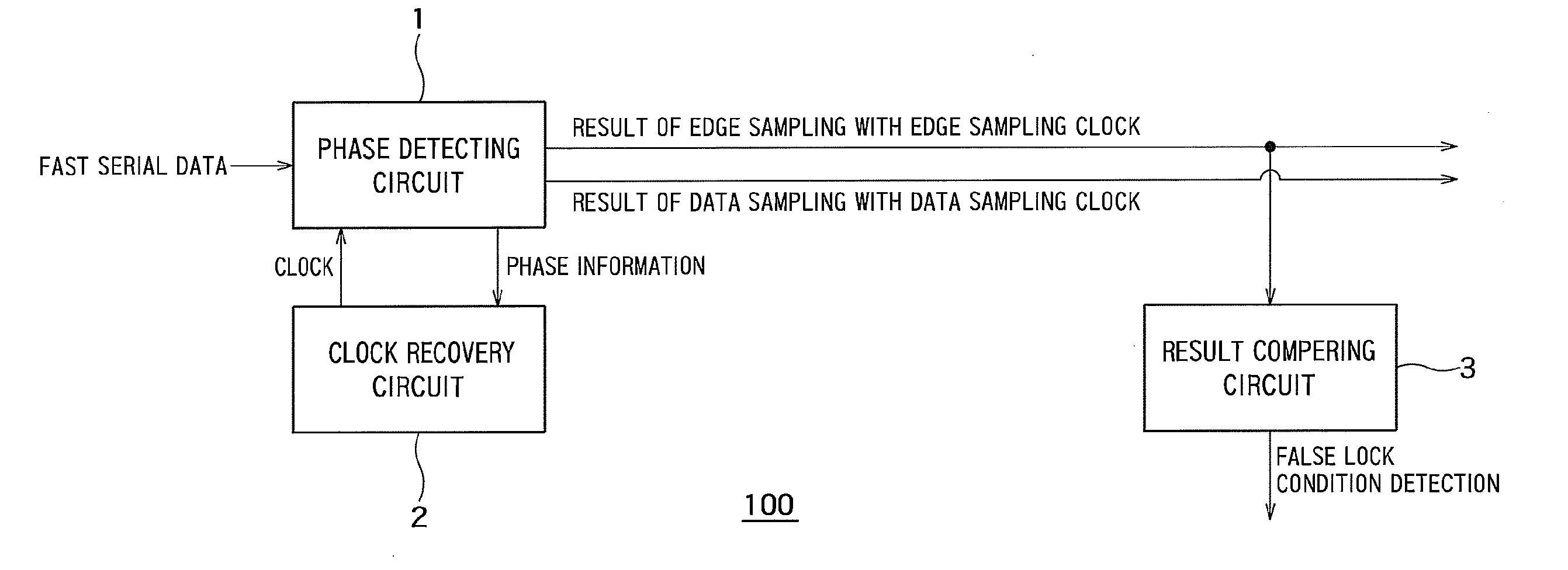
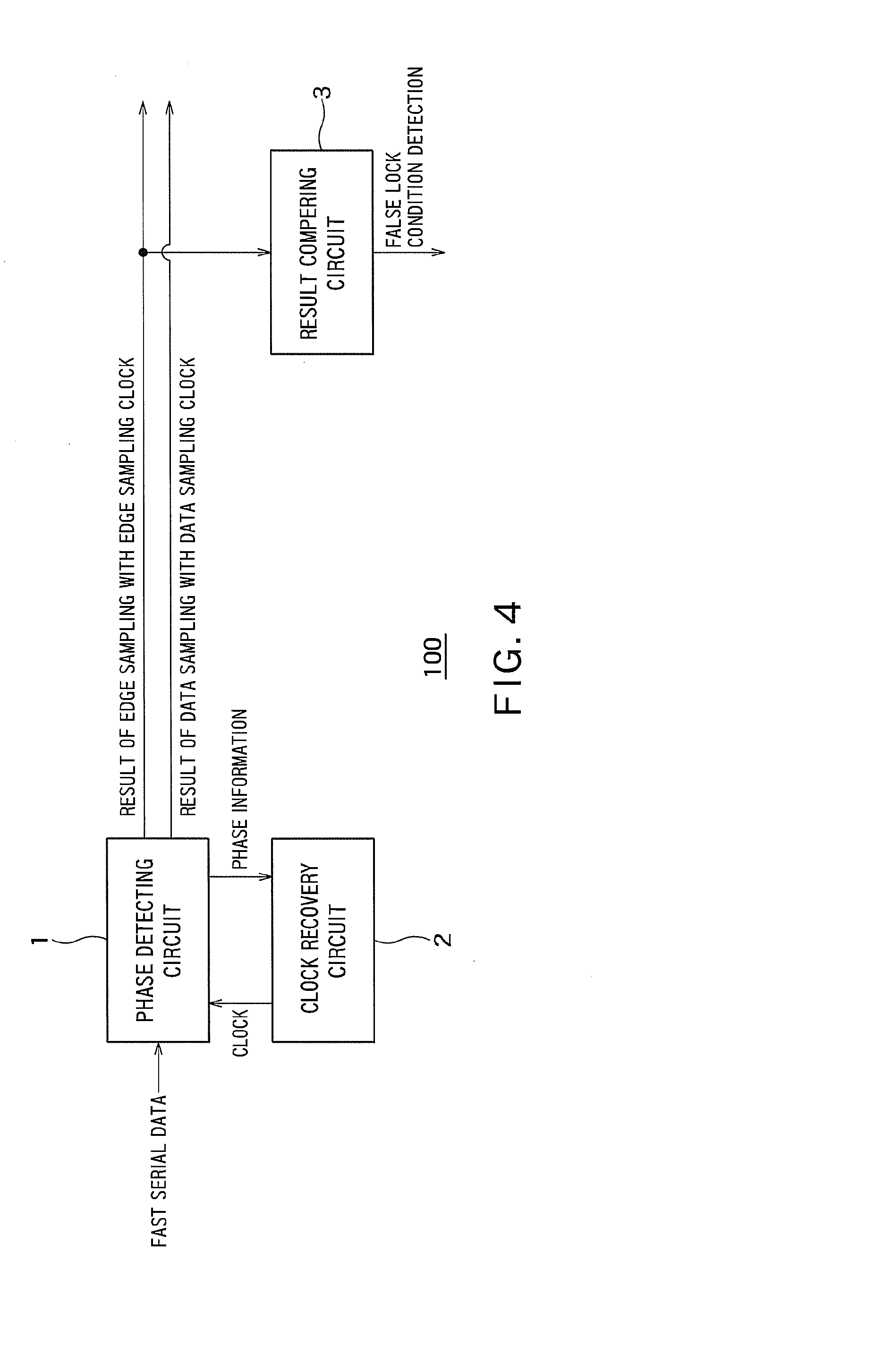
[0025]FIG. 4 is a diagram showing an example of a configuration of a CDR circuit 100 according to a first embodiment.

[0026]As shown in FIG. 4, the CDR circuit 100 is configured to output a received data signal (fast serial data encoded by an 8B10B encoder) sampled with a clock. The CDR circuit 100 is used for Peripheral Component Interconnect (PCI) Express, Serial Advanced Technology Attachment (SATA), or USB3.0 (Super Speed USB).

[0027]The CDR circuit 100 includes a phase detecting circuit 1, a clock recovery circuit 2, and a result comparing circuit 3.

[0028]The clock recovery circuit 2 is configured to generate, from an external clock (not shown), a first clock as a data sampling clock with which data of the received data signal is to be sampled and a second clock as an edge sampling clock with which an edge of the received data signal is to be sampled.

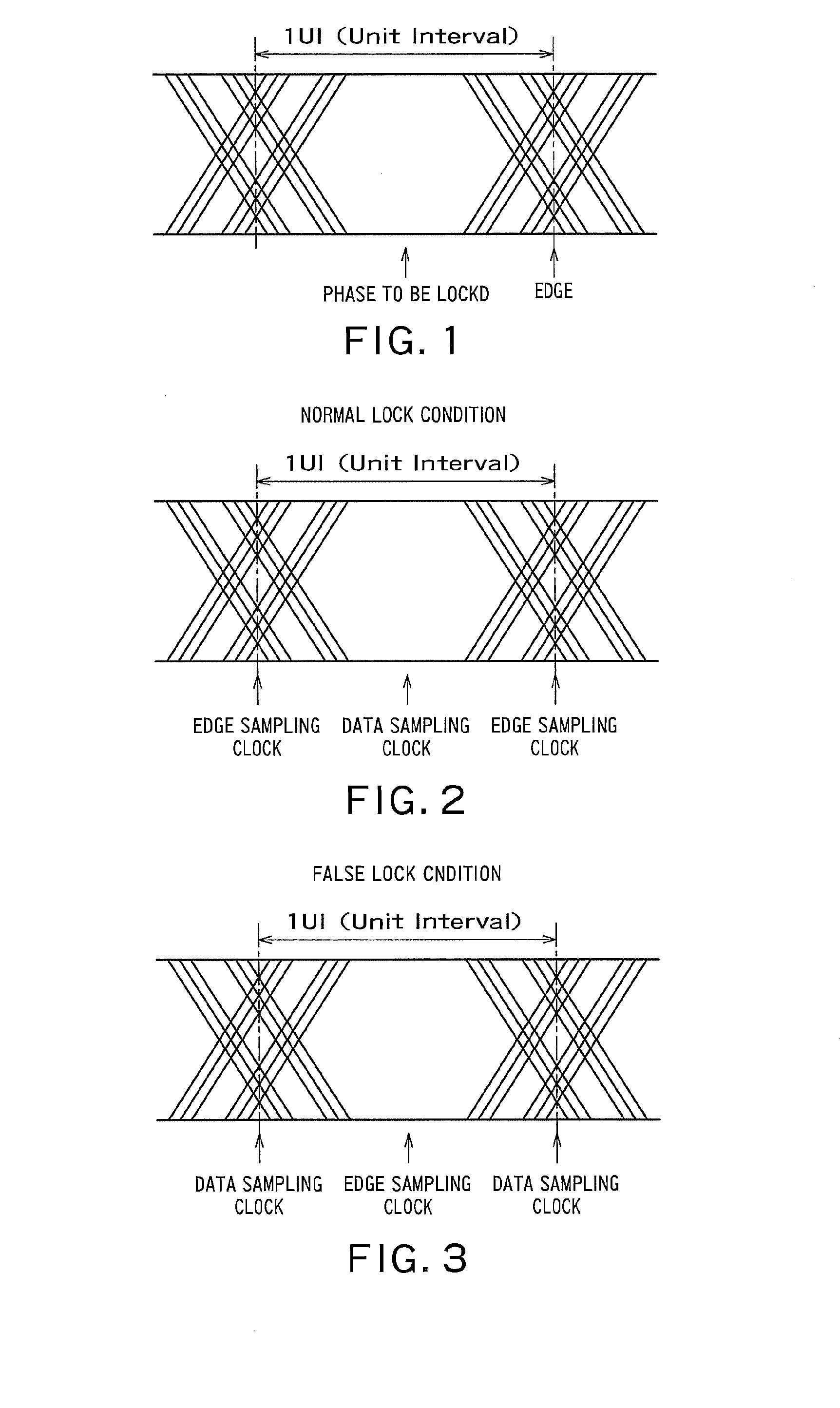
[0029]The clock recovery circuit 2 determines whether the phase of the first clock is delayed or advanced from the phase of the dat...

second embodiment

[0042]In the above first embodiment, an example of the configuration of the CDR circuit that detects the false lock condition has been described.

[0043]In a second embodiment, an example of a configuration of a CDR circuit that detects a false lock condition and recovers from the false lock condition will be described.

[0044]FIG. 5 is a diagram showing an example of a configuration of a CDR circuit 200 according to the second embodiment. In FIG. 5, the same reference numerals as those in FIG. 4 denote the same components as those in the first embodiment.

[0045]As shown in FIG. 5, the CDR circuit 200 includes the phase detecting circuit 1, the clock recovery circuit 2, and the result comparing circuit 3, as in the first embodiment.

[0046]As in the first embodiment, the result comparing circuit 3 is configured to compare the edge sampling result with the preset data pattern, and determine that the false lock condition has occurred and output the false lock condition detection signal if th...

third embodiment

[0059]In the above second embodiment, an example of the configuration of the CDR circuit that recovers from the false lock condition by resetting the operation of the clock recovery circuit in response to the control signal output from the external system has been described.

[0060]In a third embodiment, an example of a configuration of a CDR circuit that recovers from the false lock condition by resetting the operation of the clock recovery circuit in response to the false lock condition detection signal output from the result comparing circuit will be described.

[0061]FIG. 6 is a diagram showing an example of a configuration of a CDR circuit 300 according to the third embodiment. In FIG. 6, the same reference numerals as those in FIG. 5 denote the same components as those in the second embodiment.

[0062]As shown in FIG. 6, the CDR circuit 300 includes the phase detecting circuit 1, the clock recovery circuit 2, and the result comparing circuit 3, as in the second embodiment.

[0063]As i...


PUM


Abstract

A CDR circuit includes a clock recovery circuit that generates, from an external clock, a first clock with which data of a received data signal is to be sampled and a second clock with which an edge of the received data signal is to be sampled and adjusts phases of the first clock and the second clock. The CDR circuit includes a phase detecting circuit that outputs a result of sampling of the received data signal with the first clock as a data sampling result and a result of sampling of the received data signal with the second clock as an edge sampling result. The CDR circuit includes a result comparing circuit that determines that a false lock condition has occurred and outputs a false lock condition detection signal if the edge sampling result matches with the data pattern.

Description

CROSS-REFERENCE TO RELATED APPLICATION[0001]This application is based upon and claims the benefit of priority from the prior Japanese Patent Application No. 2011-207557, filed on Sep. 22, 2011, the entire contents of which are incorporated herein by reference.BACKGROUND[0002]1. Field[0003]Embodiments described herein relate generally to a Clock Data Recovery (CDR) CIRCUIT.[0004]2. Background Art[0005]Conventional CDR circuits used for fast serial data transmission can fall into a false lock condition because of the nature of their circuit characteristics.BRIEF DESCRIPTION OF THE DRAWINGS[0006]FIG. 1 is an eye pattern of a received data signal including a deterministic jitter, showing a phase to be locked;[0007]FIG. 2 is an eye pattern of a received data signal including a deterministic jitter, showing a normal lock condition;[0008]FIG. 3 is an eye pattern of a received data signal including a deterministic jitter, showing a false lock condition;[0009]FIG. 4 is a diagram showing an e...

Claims


Application Information

Patent Timeline
Patent Type & Authority Applications(United States)
IPC IPC(8): H03L7/06
CPCH03L7/0807H04L7/033H04L7/0083H03L2207/14
Inventor SATO, KIYOHITO
Owner KK TOSHIBA
Learn More