Liquid crystal display and manufacturing method thereof

a technology of liquid crystal display and manufacturing method, which is applied in the direction of optics, semiconductor devices, instruments, etc., can solve the problems of deteriorating display quality, alignment errors, and difficulty in correctly aligning pixel electrodes and color filters, so as to simplify the manufacturing process and prevent reflow. , the effect of improving the process margin

Active Publication Date: 2013-03-28
SAMSUNG DISPLAY CO LTD
View PDF1 Cites 39 Cited by
  • Summary
  • Abstract
  • Description
  • Claims
  • Application Information

AI Technical Summary

Benefits of technology

[0031]According to an exemplary embodiment of the invention, the light blocking member and the column spacer are simultaneously formed such that the reflow may be prevented, and the process margin may be improved while simplifying the manufacturing process.

Problems solved by technology

However, when the pixel electrodes and the color filters are formed on the different display panels, it is difficult to correctly align the pixel electrodes and the color filters such that an alignment error may be generated.
If the cell gap is not uniform, a uniform image is not displayed on the whole screen such that the display quality is deteriorated.
As described above, if the reflow is generated in the spacer manufacturing process, a taper of the spacer is deteriorated such that a process margin becomes poor, and a compression characteristic of the spacer to maintain the cell gap is deteriorated by an external impact.

Method used


Image

  • Liquid crystal display and manufacturing method thereof
  • Liquid crystal display and manufacturing method thereof
  • Liquid crystal display and manufacturing method thereof

Examples


Embodiment Construction

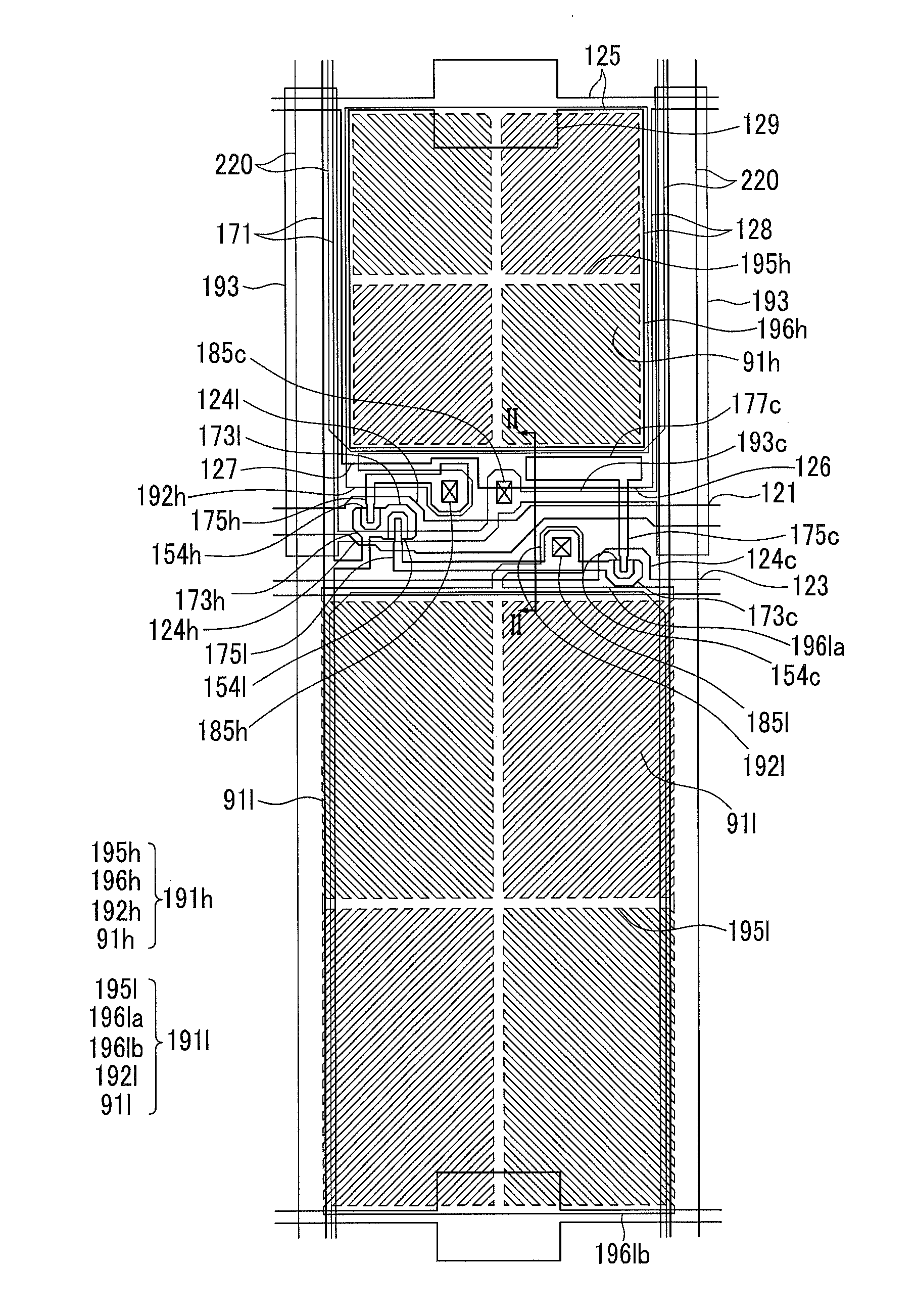
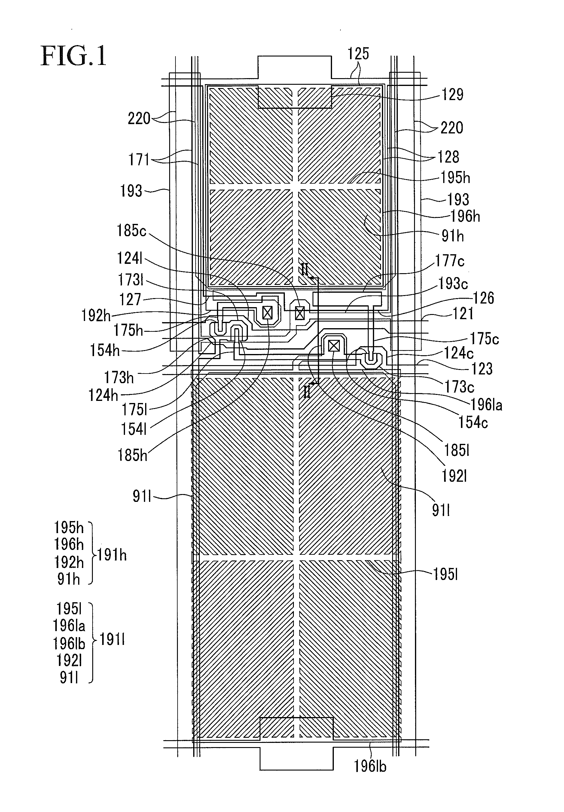
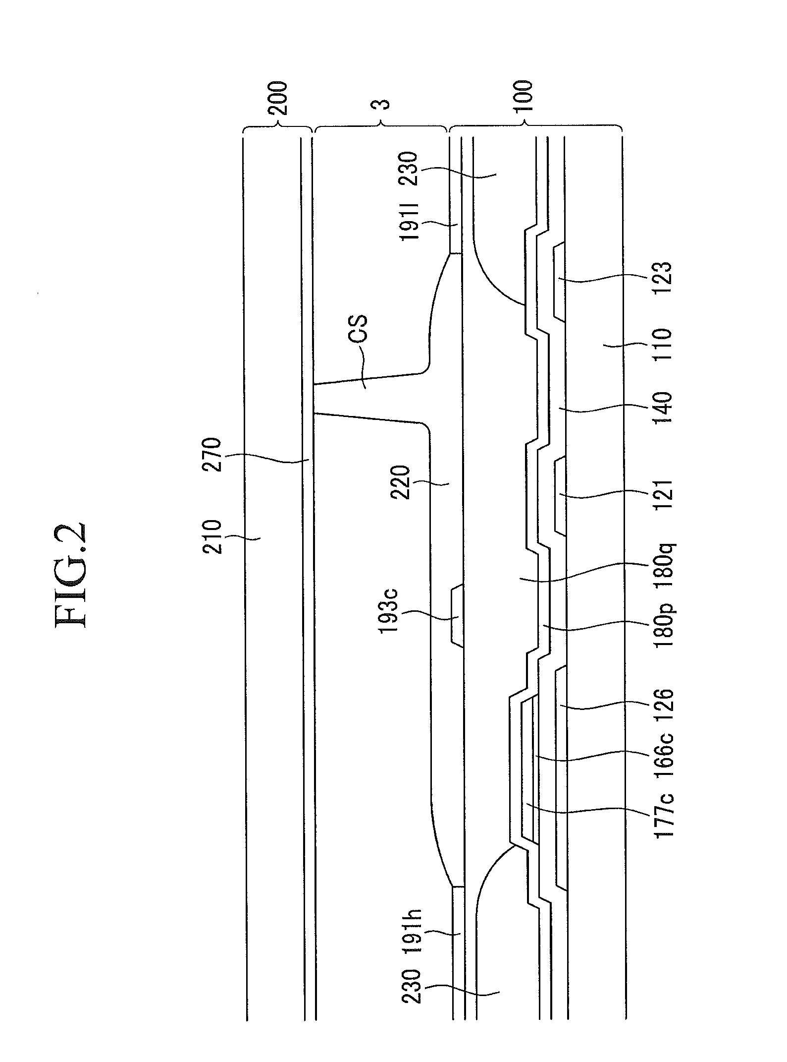
[0040]Exemplary embodiments of the invention will be described in detail with reference to the accompanying drawings. However, the invention is not limited to exemplary embodiments described herein, but may be embodied in other forms. Rather, exemplary embodiments described herein are provided to thoroughly and completely understand the disclosed contents and to sufficiently transfer the ideas of the invention to a person of ordinary skill in the art.

[0041]In the drawings, the thickness of layers and regions is exaggerated for clarity. It is to be noted that when a layer is referred to as being “on” another layer or substrate, it can be directly formed on another layer or substrate or can be formed on another layer or substrate through a third layer interposed therebetween. In contrast, when an element is referred to as being “directly on” another element or layer, there are no intervening elements or layers present. As used herein, “connected” includes physically and / or electricall...


PUM

PropertyMeasurementUnit
angleaaaaaaaaaa
angleaaaaaaaaaa
energyaaaaaaaaaa

Abstract

A manufacturing method of a liquid crystal display includes: forming a thin film transistor on a first substrate; forming a color filter on the thin film transistor; forming a pixel electrode on the color filter; and forming a light blocking member including a column spacer protruded from the light blocking member on the color filter. The forming the light blocking member uses a mask including a first region, a second region, and a third region. The first region passes light generated from a light exposer, the second region includes a blocking filter layer which selectively passes the light generated from the light exposer, and the third region blocks the light generated from the light exposer.

Description

[0001]This application claims priority to Korean Patent Application No. 10-2011-0095746 filed on Sep. 22, 2011, and all the benefits accruing therefrom under 35 U.S.C. §119, the entire contents of which are incorporated herein by reference.BACKGROUND OF THE INVENTION[0002](a) Field of the Invention[0003]The invention relates to a liquid crystal display and a manufacturing method thereof.[0004](b) Description of the Related Art[0005]Among display panels, a liquid crystal display (“LCD”) is one of flat panel displays that is being widely used, and includes two display panels in which field generating electrodes such as a pixel electrode and a common electrode, etc., are formed, and a liquid crystal (“LC”) layer disposed therebetween. The LCD displays images by applying voltages to the field-generating electrodes to generate an electric field in the LC layer that determines the orientations of LC molecules therein to adjust polarization of incident light.[0006]Among the liquid crystal ...

Claims


Application Information

Patent Timeline
Patent Type & Authority Applications(United States)
IPC IPC(8): G02F1/1335H01L33/08
CPCG02F1/13394G02F2001/136222G02F1/136209G02F1/136222G02F1/1335G02F1/1337G02F1/1339G02F1/133305G02F1/133512G02F1/133707G02F1/133788G02F1/1368
Inventor KIM, GWAN-SOOHUH, CHULKANG, DONG-UK
Owner SAMSUNG DISPLAY CO LTD
Why Eureka
Try Eureka