Semiconductor device and method of manufacturing the same

a semiconductor device and semiconductor technology, applied in the direction of semiconductor devices, basic electric elements, electrical apparatus, etc., can solve the problems of unnecessarily increasing process costs, suppressing the improvement of device performance, and difficult application of drain contacts to sources/drains formed by non-si high-mobility materials, etc., to improve the electrical performance and reliability of semiconductor devices, improve the carrier mobility in a channel region, and save process

Active Publication Date: 2013-04-11
INST OF MICROELECTRONICS CHINESE ACAD OF SCI
View PDF2 Cites 29 Cited by
  • Summary
  • Abstract
  • Description
  • Claims
  • Application Information

AI Technical Summary

Benefits of technology

[0008]Therefore, an object of the present invention is to further improve the carrier mobility in a channel region so as to improve the electrical performance and reliability of the semiconductor device while saving process and reducing the cost at the same time.
[0022]In accordance with the semiconductor device and the manufacturing method thereof in the present invention, forming the device channel region by filling the trench with epitaxial high-mobility materials in a gate last process can enhance the carrier mobility in the channel region, thereby the device response speed is substantially improved and the device performance is greatly enhanced. Furthermore, traditional materials for substrate are still used for the source / drain areas of the device to facilitate usage of a gate last process, thereby enhancing the performance while reducing the cost at the same time.

Problems solved by technology

Actually, it is enough to improve the device response speed by increasing the carrier mobility in the channel region only, and the process cost will be unnecessarily increased if the source / drain areas also adopt non-Si materials.
Besides, high-mobility materials such as Ge has a resistivity higher than that of Si, causing the source-drain parasitic series resistance to be increased, thus suppressing the improvement of the device performance to some degree, but the traditional process of taking the metal silicide as source-drain contacts is also hard to be applied to the sources / drain formed by the non-Si high-mobility materials.
Overall, the existing semiconductor device with Si channel has poor performance and reliability, the carrier mobility in the channel region shall be further improved to improve the electrical performance and reliability of the semiconductor device, while the process shall be saved and the cost shall be reduced.

Method used


Image

  • Semiconductor device and method of manufacturing the same
  • Semiconductor device and method of manufacturing the same
  • Semiconductor device and method of manufacturing the same

Examples


Embodiment Construction

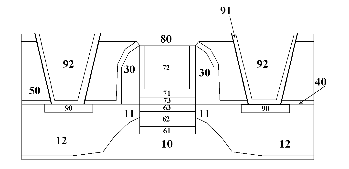
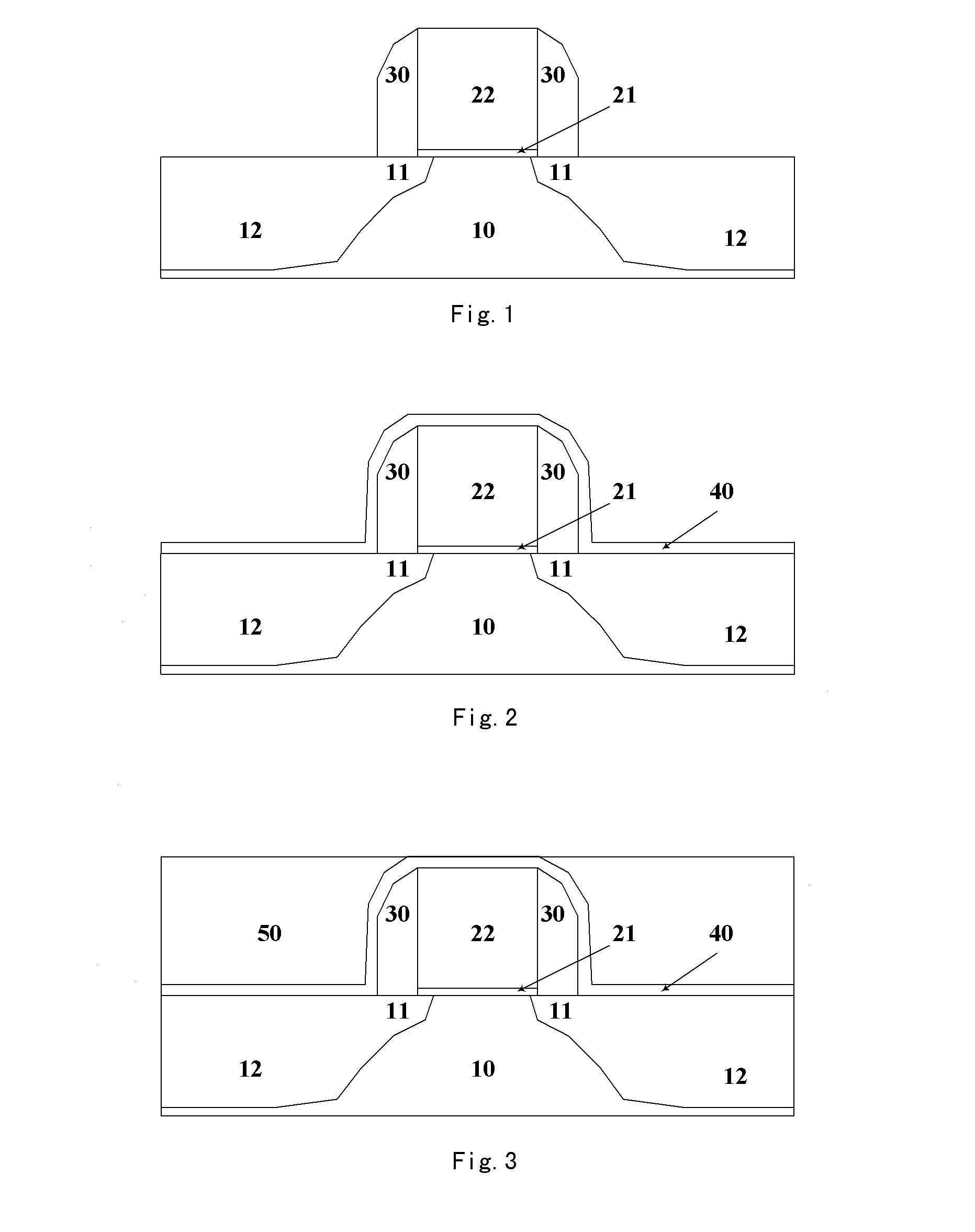
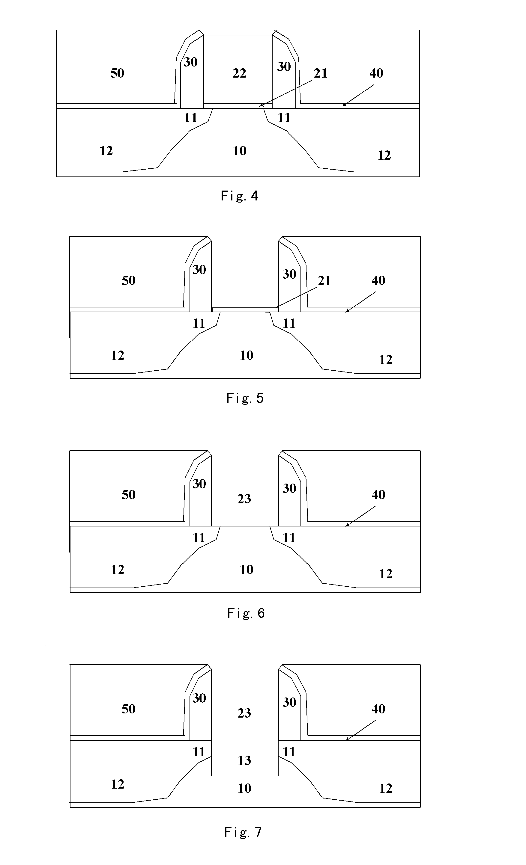
[0026]The features of the technical solutions of the present invention and the technical effects thereof are illustrated in detail in combination with the schematic embodiments with reference to the drawings, disclosed herein a semiconductor device which takes local-epitaxial, high-mobility materials as the channel and a method of manufacturing the same. It should be pointed out that like reference signs indicate like structures, the terms such as “first”, “second”, “on”, and “below” used in the present invention may be used to modify various device structures or process steps. Except for specific explanations, these modifications do not imply the spatial, sequential or hierarchical relationships of the structures of the modified device or the process steps.

[0027]First, referring to FIG. 1, a basic structure is formed, that is, a pseudo gate stack structure is formed on the substrate, source / drain areas are formed in the substrate on both sides of the pseudo gate stack structure, an...


PUM


Abstract

The present invention discloses a semiconductor device, comprising: a substrate, a channel layer epitaxially grown in the substrate, a gate stack structure on the channel layer, gate spacers on both sides of the gate stack structure, and source / drain areas on both sides of the channel layer in the substrate, characterized in that the carrier mobility of the channel layer is higher than that of the substrate. In accordance with the semiconductor device and the method of manufacturing the same in the present invention, forming the device channel region by filling the trench with epitaxial high-mobility materials in a gate last process can enhance the carrier mobility in the channel region, thereby the device response speed is substantially improved and the device performance is greatly enhanced. Furthermore, traditional materials for a substrate are still used for the source / drain areas of the device to facilitate usage of a gate last process, thereby enhancing the performance while reducing the cost at the same time.

Description

CROSS REFERENCE[0001]This application is a National Phase application of, and claims priority to, PCT Application No. PCT / CN2011 / 082002, filed on Nov. 30 , 2011, entitled ‘SEMICONDUCTOR DEVICE AND METHOD OF MANUFACTURING THE SAME’, which claimed priority to Chinese Application No. CN 201110303593.5, filed on Oct. 9, 2011. Both the PCT Application and Chinese Application are incorporated herein by reference in their entireties.FIELD OF THE INVENTION[0002]The present invention relates to a semiconductor device and method of manufacturing the same, particularly to a semiconductor device which takes local-epitaxial, high-mobility material film as the channel and a method of manufacturing the same.BACKGROUND OF THE INVENTION[0003]With continuous reduction in the size of a semiconductor device, enhancing the carrier mobility of channel becomes a very important technique. In the design of a stress layer for a substrate, different materials have different characteristics such as lattice con...

Claims


Application Information

Patent Timeline
Patent Type & Authority Applications(United States)
IPC IPC(8): H01L29/78H01L21/336
CPCH01L29/517H01L29/518H01L29/66477H01L29/1054H01L29/66545H01L29/66651H01L29/66522
Inventor WANG, GUILEI
Owner INST OF MICROELECTRONICS CHINESE ACAD OF SCI
Why Eureka
Try Eureka