Device having an avalanche photo diode and a method for sensing photons

a technology of which is applied in the field of avalanche photo diodes and avalanche photo diodes, can solve the problems of reducing the effective fill factor and the photon detection efficiency (pde), not being able to scale much below 5 m, and not being available in commercially available geiger mode cmos imagers with mega-pixels

Active Publication Date: 2013-04-25
TECHNION RES & DEV FOUND LTD +1
View PDF1 Cites 25 Cited by
  • Summary
  • Abstract
  • Description
  • Claims
  • Application Information

AI Technical Summary

Benefits of technology

[0056]The method may include maintaining an electrical field form across the p-n junction constant while allowing photo-carriers multiplications to occur within a depletion region of the APD.

Problems solved by technology

In spite of impressive progress, Geiger mode CMOS imagers with mega-pixels are still not available commercially.
This approach significantly reduces the effective fill factor and the Photon Detection Efficiency (PDE) since photo-carriers that reach the guard ring are not multiplied.
Furthermore, they cannot be scaled much below 5 μm because the depletion regions around the p-well implants expand and merge such that the active area of the SPAD is almost fully depleted.

Method used


Image

  • Device having an avalanche photo diode and a method for sensing photons
  • Device having an avalanche photo diode and a method for sensing photons
  • Device having an avalanche photo diode and a method for sensing photons

Examples


Embodiment Construction

[0087]In the following detailed description, numerous specific details are set forth in order to provide a thorough understanding of the invention. However, it will be understood by those skilled in the art that the present invention may be practiced without these specific details. In other instances, well-known methods, procedures, and components have not been described in detail so as not to obscure the present invention.

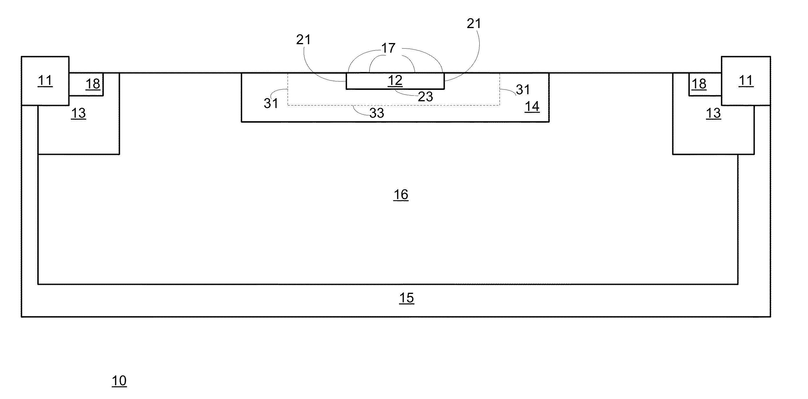
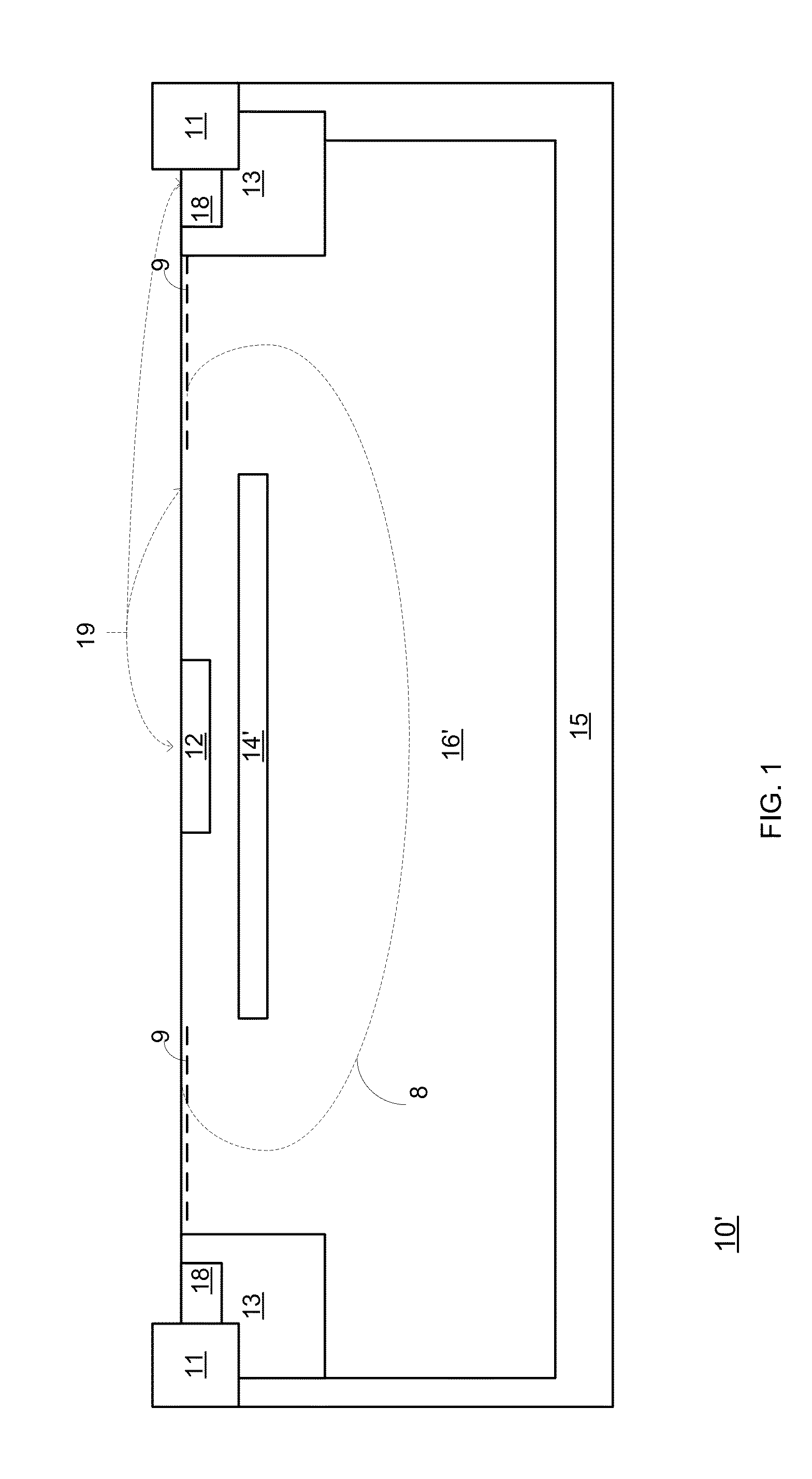
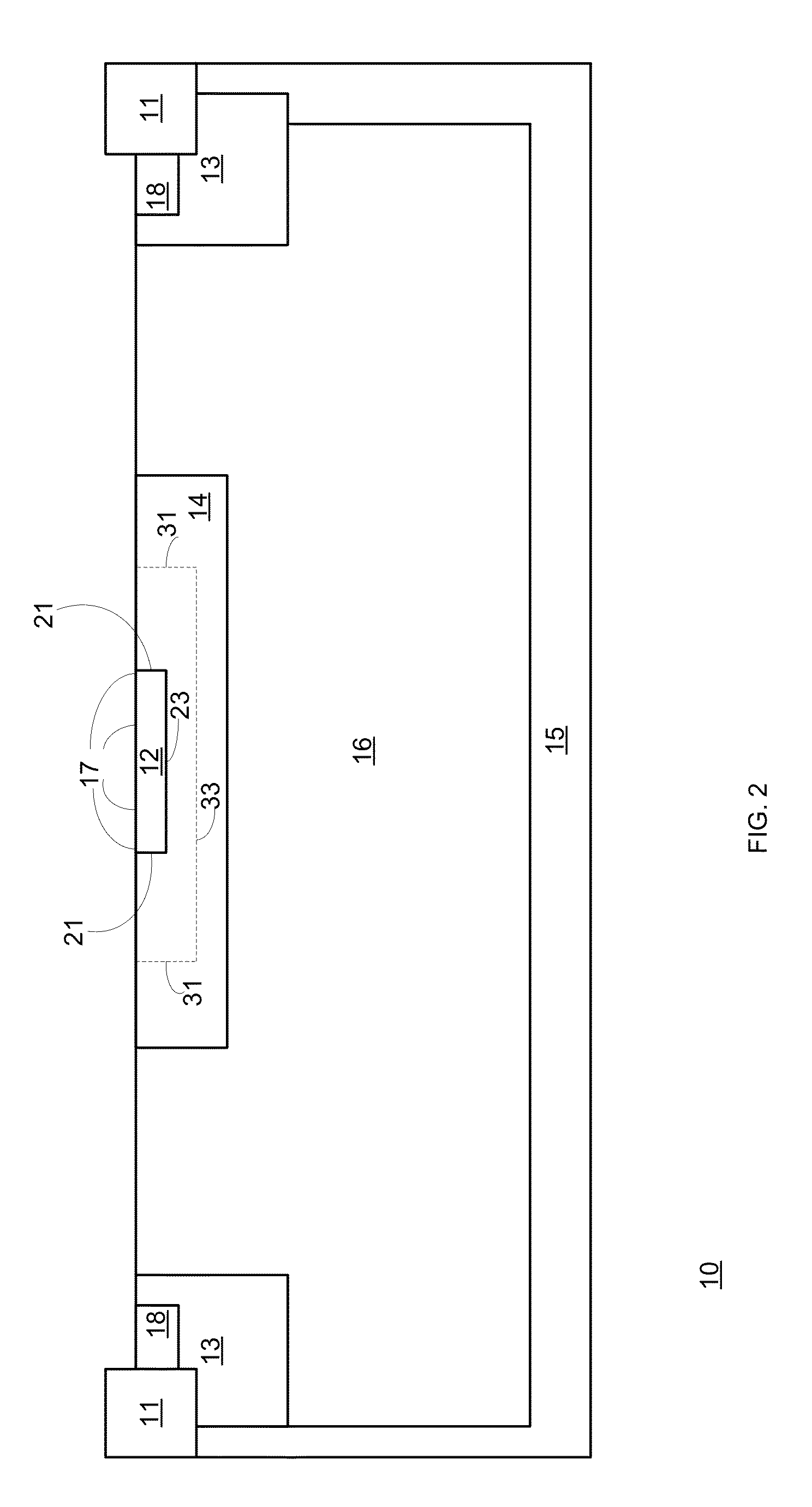
[0088]There is provided a high-performance APD that can be manufactured by CMOS technologies. The CMOS technologies may include but are not limited to low-voltage 0.18 micron CMOS technology.

[0089]The APD may be Geiger mode and act as a SPAD. Alternatively, the APD may be biased by a bias voltage that is below a breakdown bias of the APD and may operate in a linear mode. In any case—the APD should be biased to facilitate a multiplication of photo-carriers generated in the depletion region.

[0090]According to an embodiment of the invention the APD may include (a) a ...


PUM


Abstract

A semiconductor device that may include an avalanche photodiode (APD), the APD may include: a first doped region of a first polarity; a buried guard ring of a second polarity, the second polarity is opposite to the first polarity, the buried guard ring is spaced apart from the first doped region and is positioned below the first doped region; a well of the second polarity, wherein the well interfaces the first doped region to form a p-n junction; and a second doped region of the second polarity, the second doped region is spaced apart from the first doped region.

Description

[0001]This application claims priority of U.S. provisional patent serial date 61 / 536,076 filing date Sep. 19, 2011 which is incorporated herein by reference.BACKGROUND OF THE INVENTION[0002]Highly demanding photonic applications require the acquisition of images at very low light-level conditions and at high speed. Only Geiger mode CMOS imager, where the sensor in each pixel is Single Photon Avalanche Photodiode (SPADs), may meet the requirements for exceptional time resolution and ultimate optical sensitivity simultaneously. In spite of impressive progress, Geiger mode CMOS imagers with mega-pixels are still not available commercially.[0003]It is known that a better insight in the evolution of the design and fabrication technology of SPADs up to the most recent results may be gained by looking at it in historical perspective, following the various reported designs and the two fabrication technologies, i.e., standard high-voltage CMOS (HV-CMOS) and dedicated CMOS-compatible technolo...

Claims


Application Information

Patent Timeline
Patent Type & Authority Applications(United States)
IPC IPC(8): H01L31/024H01L31/107
CPCH01L31/107H01L31/024
Inventor NEMIROVSKY, YAELSAVUSKAN, VITALIBAR-LEV SHEFI, SHARONBROUK, IGORVISOKOLOV, GILFENIGSTEIN, AMOSLEITNER, TOMER
Owner TECHNION RES & DEV FOUND LTD
Why Eureka
Try Eureka