Solid-state imaging device, members for the same, and imaging system

a technology of solid-state imaging and imaging system, which is applied in the direction of material analysis, radiological control devices, instruments, etc., can solve problems such as degrading sensitivity, and achieve the effect of reducing the possibility of metal pollution and restricting the occurren

Active Publication Date: 2013-04-25
CANON KK
View PDF2 Cites 19 Cited by
  • Summary
  • Abstract
  • Description
  • Claims
  • Application Information

AI Technical Summary

Benefits of technology

[0011]The solid-state imaging device according to the present invention can provide a pad capable of restraining the occurrence of inferior connection with an external terminal and reducing the possibility of occurrence of metal pollution.
[0012]Further features and aspects of the present invention will become apparent from the following detailed description of exemplary embodiments with reference to the attached drawings.

Problems solved by technology

However, reducing the size of a pixel decreases the light-receiving area of a photoelectric conversion element for light detection included in the pixel, resulting in degraded sensitivity.

Method used


Image

  • Solid-state imaging device, members for the same, and imaging system
  • Solid-state imaging device, members for the same, and imaging system
  • Solid-state imaging device, members for the same, and imaging system

Examples


example 1

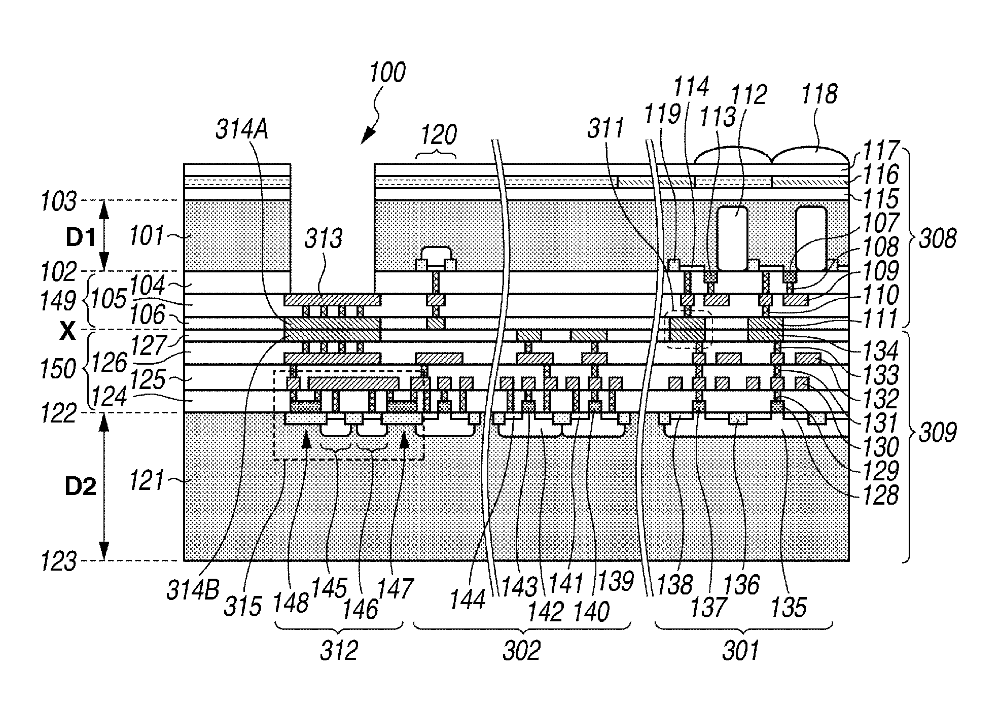
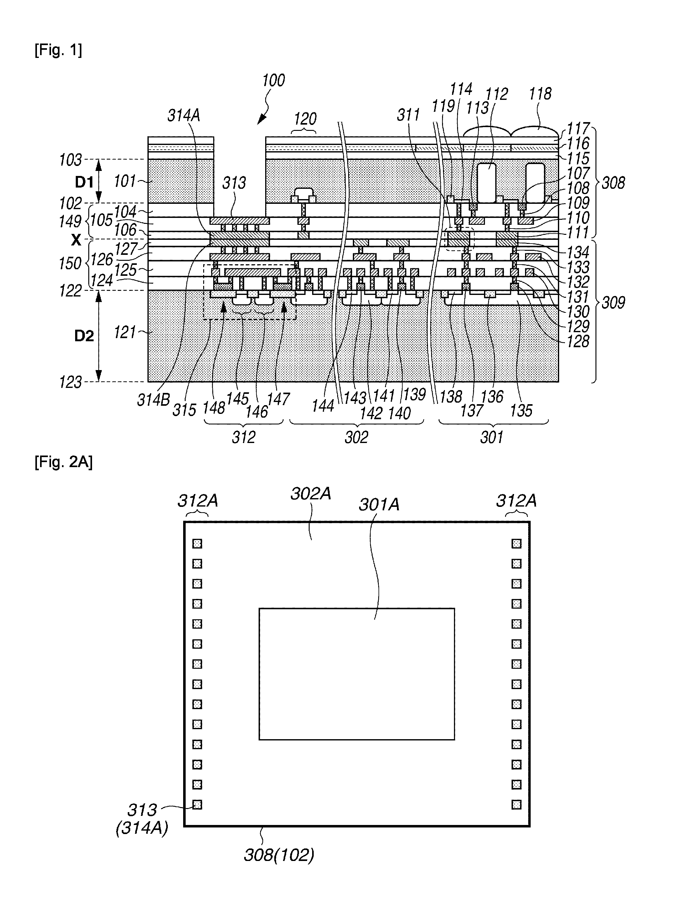
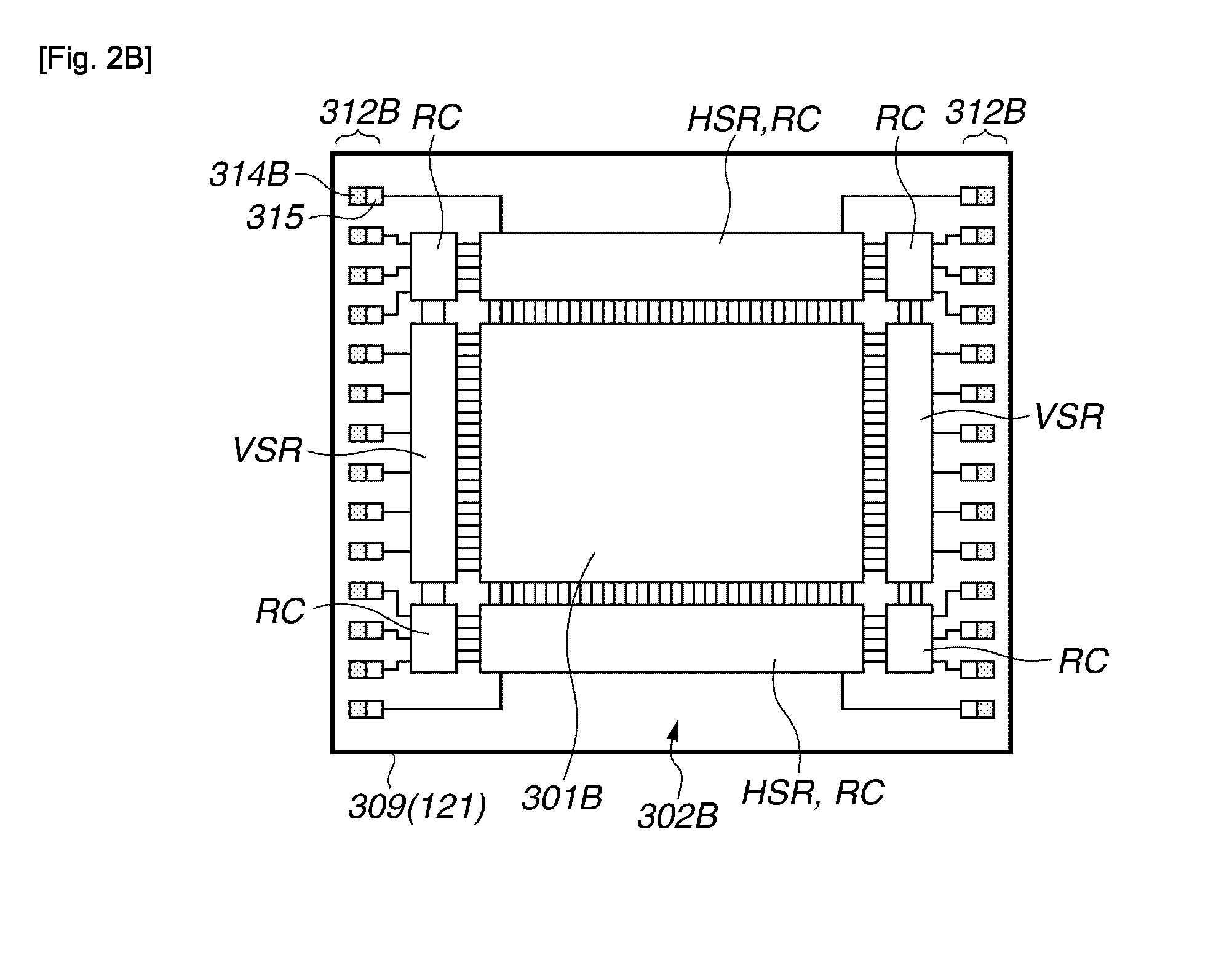
[0030]The present invention will be described in detail below with reference to the accompanying drawings. In the following descriptions of exemplary embodiments, the front face of the first substrate and the front face of the second substrate are substrate surfaces (principle planes) on which transistors are formed. For each of the first and second substrates, the face on the opposite side of the front face is the back face (read face). For each substrate, an upward direction refers to a direction from the back face to the front face, and a downward direction or depth direction refers to a direction from the front face to the back face. In the following descriptions, when the first and second substrates are bonded with each other, the back face of the second substrate is at the bottom face and the back face of the first substrate is at the top.

[0031]A first exemplary embodiment of the present invention will be described below with reference to FIGS. 1 to 6A and 6B.

[0032]First of al...


PUM


Abstract

The present invention provides a solid-state imaging device including a pad capable of reducing inferior connection with an external terminal. The solid-state imaging device includes a first substrate provided, on its front face, with photoelectric conversion elements, a first wiring structure, a second substrate provided, on its front face, with at least a part of peripheral circuits, and a second wiring structure. The first substrate, the first wiring structure, the second wiring structure, and the second substrate are provided in this order. The first wiring structure includes a wiring layer including wirings made mainly of copper. The second wiring structure includes a wiring layer including wirings made mainly of copper. Wirings made mainly of copper in the wiring layer in the first wiring structure are bonded with wirings made mainly of copper in the wiring layer in the second wiring structure. The solid-state imaging device includes a pad formed of a conductive element made mainly of aluminum.

Description

TECHNICAL FIELD[0001]The present invention relates to a solid-state imaging device and more particularly to a pad.BACKGROUND ART[0002]With charge-coupled device (CCD)-type and amplifier-type solid-state imaging devices for digital still cameras and camcorders, miniaturization of pixels has been demanded to obtain high definition images. However, reducing the size of a pixel decreases the light-receiving area of a photoelectric conversion element for light detection included in the pixel, resulting in degraded sensitivity.[0003]Patent Document 1 discloses an amplifier-type complementary metal-oxide semi-conductor (CMOS) solid-state imaging device fabricated by bonding a first substrate provided with photoelectric conversion elements and transfer transistors, and a second substrate provided with other circuits to ensure the light-receiving area of a photo-electric conversion element. The first and second substrates are bonded with each other by using copper bonding pads.[0004]Further,...

Claims


Application Information

Patent Timeline
Patent Type & Authority Applications(United States)
IPC IPC(8): H01L27/146
CPCH01L23/481H01L27/14632H01L27/14638H01L27/1464H01L2924/0002H01L27/14636H01L2924/00H01L27/14609H01L27/14634H01L27/1469
Inventor KOBAYASHI, MASAHIRO
Owner CANON KK
Why Eureka
Try Eureka