Multilayered circuit type antenna package

a multi-layer circuit and antenna technology, applied in antennas, semiconductor/solid-state device details, modular arrays, etc., can solve the problems of high manufacturing cost of millimeter band communication technology, difficult cable connection method, high price, etc., and achieve the effect of minimizing the number of stacked layers

Active Publication Date: 2013-04-25
SAMSUNG ELECTRONICS CO LTD
View PDF3 Cites 240 Cited by
  • Summary
  • Abstract
  • Description
  • Claims
  • Application Information

AI Technical Summary

Benefits of technology

[0009]Exemplary embodiments provide a multilayered antenna package for millimeter band communication in which the number of stacked layers is minimized.

Problems solved by technology

Unlike the related art near field or middlefield communication methods that use cables to provide connections, in millimeter band communication it is difficult to use a cable connection method due to the high frequencies involved.
Also, millimeter band-exclusive signal cables are usually several tens of dollars, and thus, the high price is an obstacle for commercialization of 60 GHz communication modules.
In a low temperature co-fired ceramic (LTCC) process for implementing these multilayered structures, the high manufacturing costs thereof are an obstacle in commercializing millimeter band communication technology.

Method used


Image

  • Multilayered circuit type antenna package
  • Multilayered circuit type antenna package
  • Multilayered circuit type antenna package

Examples


Embodiment Construction

[0029]Exemplary embodiments will now be described more fully with reference to the accompanying drawings. In the drawings, like reference numerals denote like elements, and the sizes of elements in the drawings may be exaggerated for clarity and convenience.

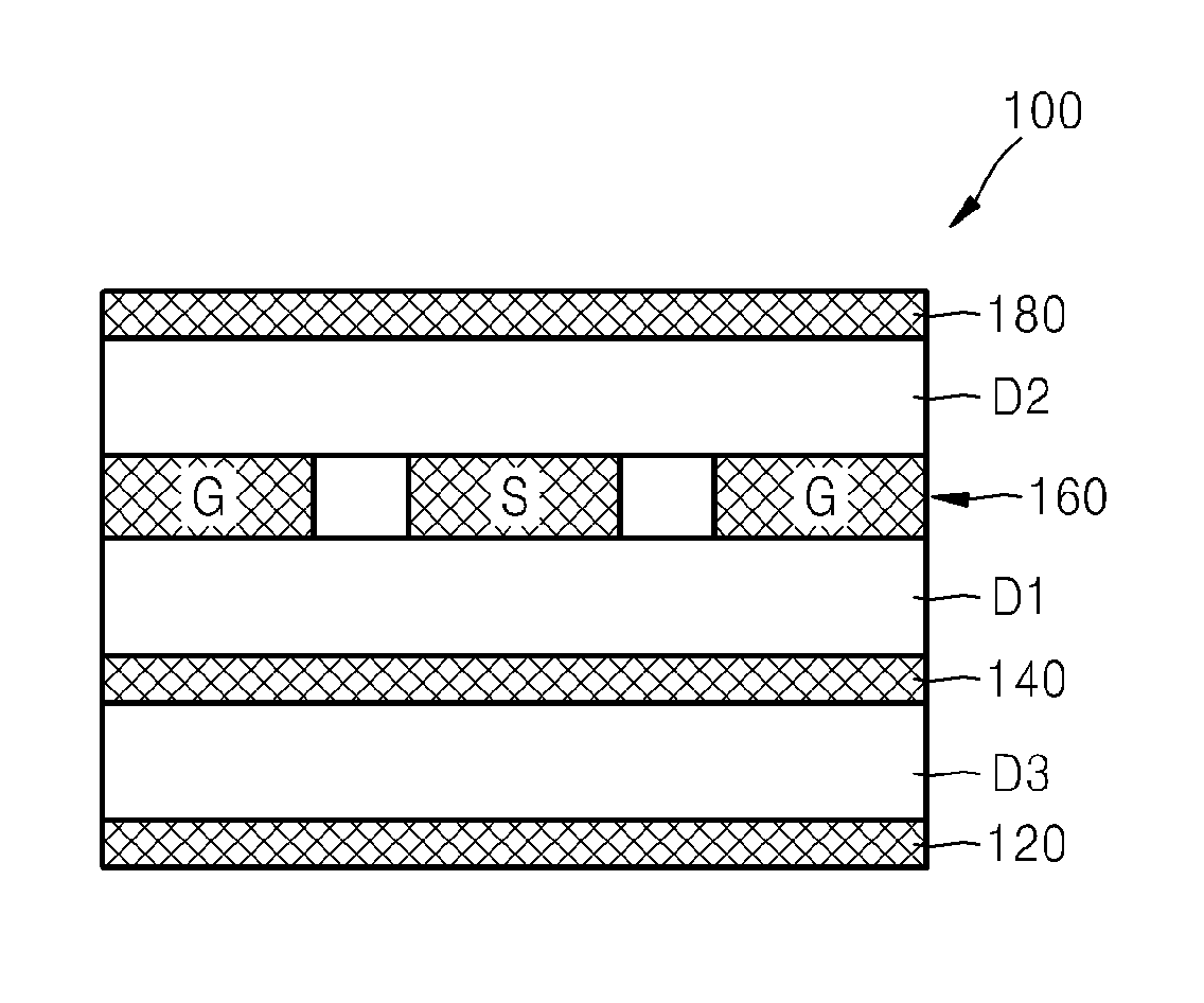
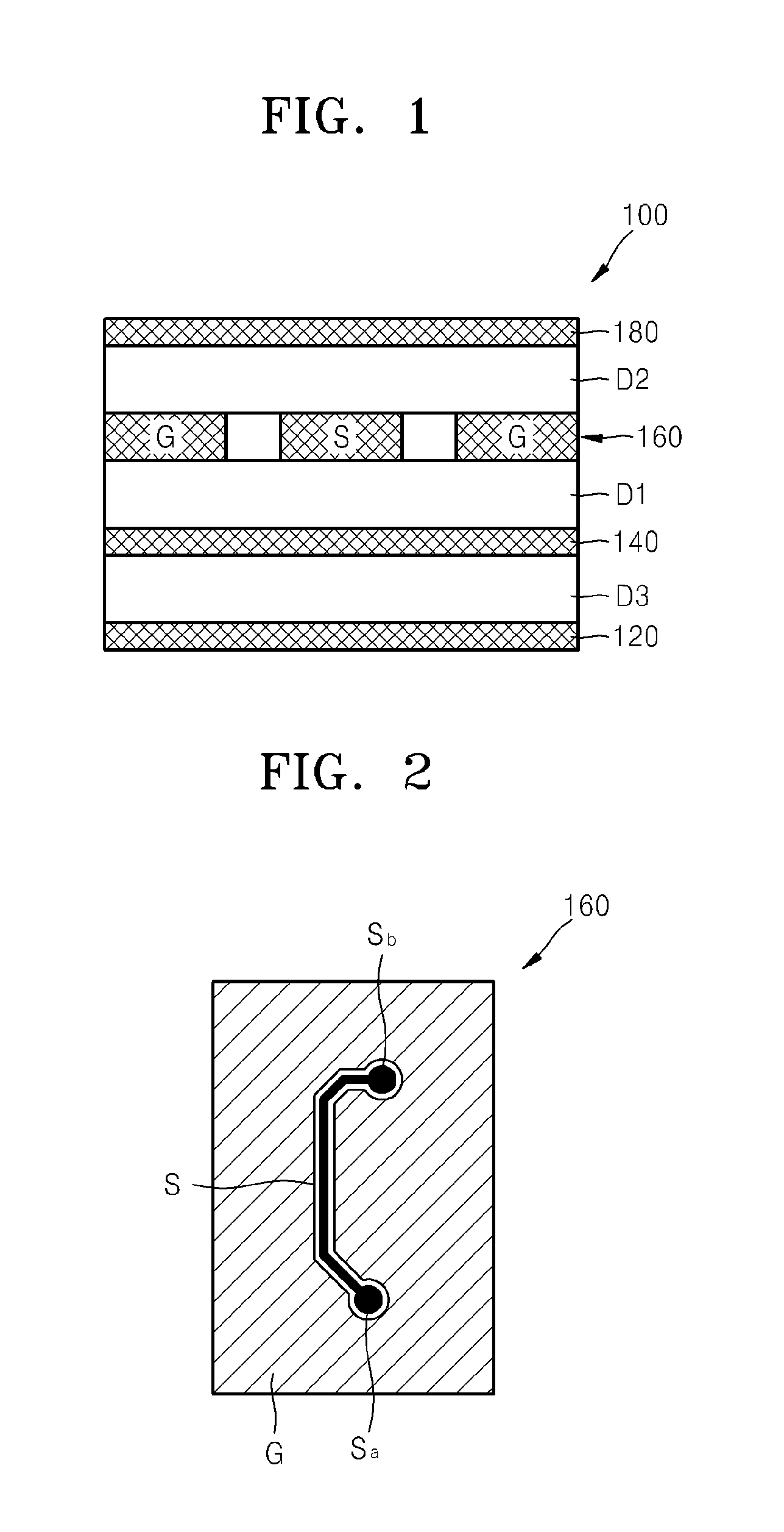
[0030]FIG. 1 is a schematic diagram schematically illustrating an arrangement of a multilayered antenna package in which the number of stacked layers is minimized, according to an exemplary embodiment. FIG. 2 is a plan view illustrating an exemplary arrangement of a signal line S and a grounding portion G of a coplanar waveguide (CPW) layer of the multilayered antenna package of FIG. 1.

[0031]Referring to FIG. 1, a multilayered antenna package 100 includes a CPW layer 160 formed on a first dielectric layer D1, and an antenna portion 180 formed on the CPW layer 160, and a radio frequency integrated circuit (RFIC) interface layer 140 formed under the CPW layer 160. The antenna portion 180 is formed on a second dielectric layer D2 di...


PUM


Abstract

A multilayered antenna package including: a radio frequency integrated circuit (RFIC) interface layer that is configured to transmit a radio frequency (RF) signal; a first dielectric layer that is disposed on the RFIC interface layer; a coplanar waveguide layer that is disposed on the first dielectric layer and is configured to receive the RF signal transmitted by RFIC layer; a second dielectric layer disposed on the coplanar waveguide layer; and an antenna portion that is disposed on the second dielectric layer and is configured to irradiate a signal that is transmitted from the coplanar waveguide layer.

Description

CROSS-REFERENCE TO RELATED PATENT APPLICATION[0001]This application claims priority from Korean Patent Application No. 10-2011-0107059, filed on Oct. 19, 2011, in the Korean Intellectual Property Office, the disclosure of which is incorporated by reference herein in its entirety.BACKGROUND[0002]1. Field[0003]Apparatuses, devices, and articles of manufacture consistent with the present disclosure relate to a multilayered antenna package for millimeter band communication.[0004]2. Description of the Related Art[0005]Millimeter band communication, which is being developed for transmission of large capacity audio / video (AV) data at high speeds on the order of gigabits per second (GBps), is capable of transmitting large capacity data several times faster than near field or middlefield communication methods such as Wireless Fidelity (WiFi), wireless local area network (WLAN), wireless personal area network (WPAN), etc.[0006]Unlike the related art near field or middlefield communication met...

Claims


Application Information

Patent Timeline
Patent Type & Authority Applications(United States)
IPC IPC(8): H01L23/48
CPCH01Q21/0025H01Q1/2283
Inventor HONG, WON-BINGOUDELEV, ALEXANDERBAEK, KWANG-HYUNKIM, YOUNG-HWAN
Owner SAMSUNG ELECTRONICS CO LTD
Why Eureka
Try Eureka