Radio frequency amplifier circuit

a technology of amplifier circuit and frequency, applied in the direction of amplifiers with semiconductor devices only, semiconductor/solid-state device details, etc., can solve the problems of reducing the reliability of a device, difficult heat release design, and reducing efficiency, so as to achieve high efficiency and stability.

Active Publication Date: 2013-05-02
PANASONIC SEMICON SOLUTIONS CO LTD
View PDF7 Cites 24 Cited by
  • Summary
  • Abstract
  • Description
  • Claims
  • Application Information

AI Technical Summary

Benefits of technology

[0014]The present invention relates to a radio frequency amplifier circuit including a harmonic processing circuit. In the radio amplifier circuit, output terminals of low-output transistors are connected via a resistor, and the harmonic processing circuit which has an impedance to be ideally short-circuited in a high frequency is connected to each of the low-output transistors. This enables the harmonic processing for the class-F operation or the inverse class-F operation with high efficiency and stability.

Problems solved by technology

This makes a heat-release design be difficult and decreases reliability of a device.
In the amplifier circuit, power loss causes the efficiency to decrease.

Method used


Image

  • Radio frequency amplifier circuit
  • Radio frequency amplifier circuit
  • Radio frequency amplifier circuit

Examples


embodiment 1

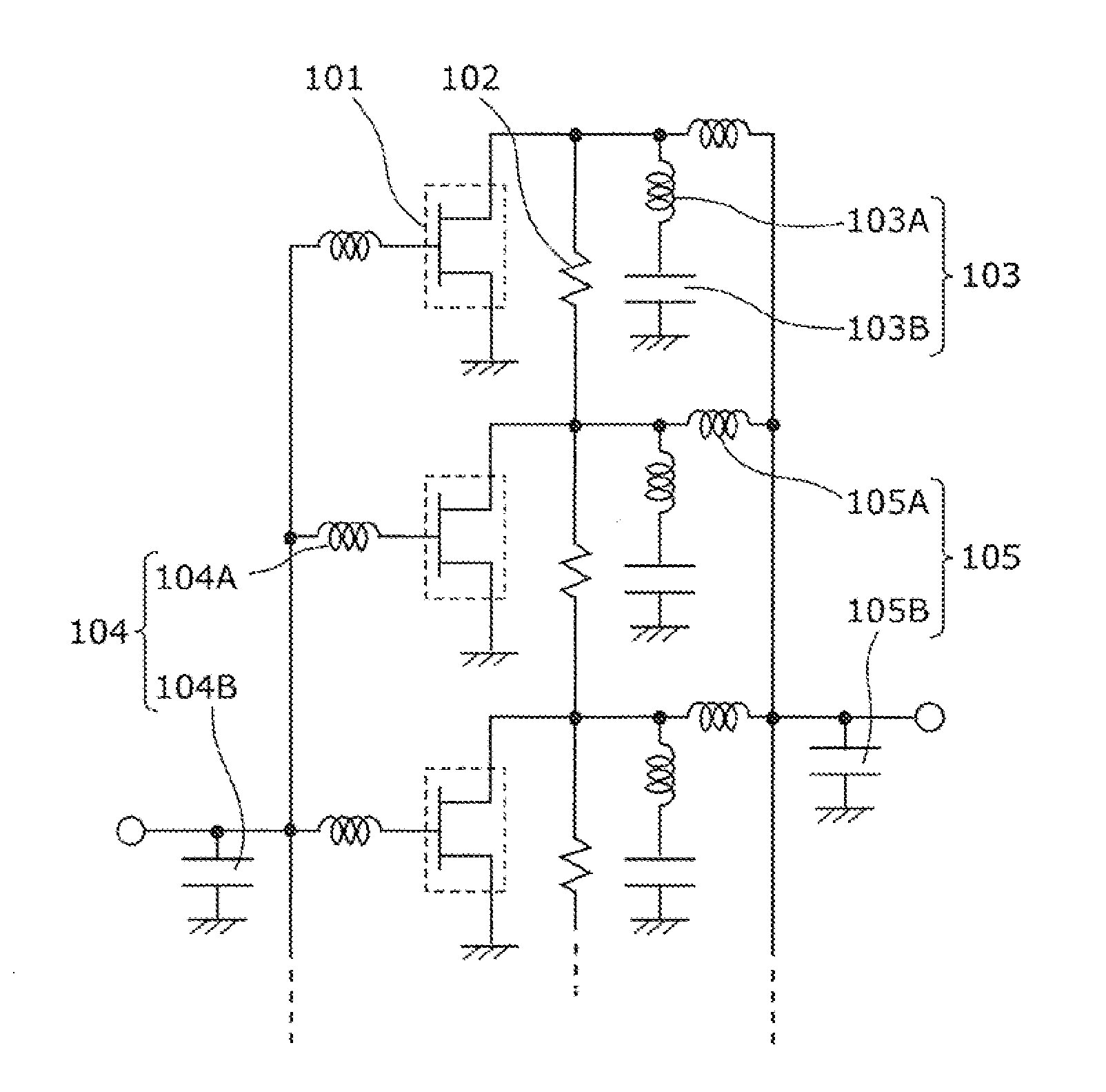
[0059]FIG. 1 is a circuit diagram which shows a radio frequency amplifier circuit according to Embodiment 1 of the present invention. The radio frequency amplifier circuit shown in FIG. 1 includes a plurality of low-output transistors 101 arranged in parallel, a resistor 102 disposed between drain output terminals of adjacent low-output transistors, a harmonic processing circuit 103 connected to each of the output terminals of the low-output transistors 101, an input-side fundamental matching circuit 104, and an output-side fundamental matching unit 105.

[0060]Each of the low-output transistors 101 is a first transistor which has a narrow gate width Wg, and outputs an amplified radio frequency signal. The amplified radio frequency signal passes through the output fundamental matching circuit 105, and is collected to be a high output. The high output is supplied from an output terminal of the radio frequency amplifier circuit.

[0061]The resistor 102 is an output-side resistor which con...

embodiment 2

[0093]FIG. 3 is a circuit diagram which shows a radio frequency amplifier circuit according to Embodiment 2 of the present invention. The radio frequency amplifier circuit shown in FIG. 3 includes a plurality of low-output transistors 301 connected in parallel, a resistor 302 arranged between drain output terminals of the adjacent low-output transistors 301, a harmonic processing circuit 303 connected to each of the drain output terminals of the low-output transistors 301, an input-side fundamental matching circuit 304, an output-side fundamental matching circuit 305, a resistor 311 arranged between gate input terminals of the adjacent low-output transistors 301, a harmonic processing circuit 312 connected to each of the gate input terminals of the low-output transistors 301.

[0094]The radio frequency amplifier circuit shown in FIG. 3 according to Embodiment 2 is different from the radio frequency amplifier circuit shown in FIG. 1 in a point that the resistor 311 and the harmonic pro...

embodiment 3

[0115]FIG. 5 is a circuit diagram which shows a radio frequency amplifier circuit according to Embodiment 3 of the present invention. The radio frequency amplifier circuit shown in FIG. 5 includes a plurality of low-output transistors 501A and a plurality of low-output transistors 501B both of which are connected in parallel, a resistor 502 arranged between drain output terminals of the low-output transistors 501A and 501B which are adjacent to each other, the harmonic processing circuit 503 connected to each of the drain output terminals of the low-output transistors 501B, the input-side fundamental matching circuit 504, and the output-side fundamental matching circuit 505.

[0116]The radio frequency amplifier circuit according to Embodiment 3, which is shown in FIG. 5, is different from the radio frequency amplifier circuit in FIG. 1 in a point that the resistor 502 and the harmonic processing circuit 503 that are arranged in the output side are not connected to each of the low-outp...


PUM


Abstract

A radio frequency amplifier circuit includes: low-output transistors, each of which includes an input terminal, an output terminal, and a ground terminal, and amplifies a radio frequency signal; a harmonic processing circuit provided for each of the low-output transistors to be connected to the output terminal of the low-output transistor, and processing a secondary harmonic included in an amplified radio frequency signal, and a resistor connected to the output terminal of each of the low-output transistors. The input terminal of each of the low-output transistors is connected to an input terminal of the radio frequency amplifier circuit via an inductor, and the output terminal of each of the low-output transistors is connected to the other output terminal via the resistance and is further connected to an output terminal of the radio frequency amplifier circuit via an inductor.

Description

TECHNICAL FIELD[0001]The present invention relates to radio frequency amplifier circuits including harmonic processing circuits, and particularly to a radio frequency amplifier circuit including a class-F circuit.BACKGROUND ART[0002]Improvement in power added efficiency (PAE) of a radio frequency amplifier circuit directly relates to reduction in power consumption of a device. Accordingly, the PAE is a very important property. In a high-output amplifier circuit, supplied power is converted into heat due to power consumption and a low PAE. This makes a heat-release design be difficult and decreases reliability of a device.[0003]Conventionally, in order to cause the radio frequency amplifier circuit to operate at high efficiency, a device which includes a class-F circuit and an inverse class-F circuit has been generally used. Accordingly, mechanisms of these high efficiency circuits are known. In the amplifier circuit, power loss causes the efficiency to decrease. In order to prevent ...

Claims


Application Information

Patent Timeline
Patent Type & Authority Applications(United States)
IPC IPC(8): H03F3/193
CPCH03F3/193H03F3/211H01L2924/1305H01L2924/3011H01L2924/30107H01L2224/49175H01L2224/48091H01L2223/6655H01L2223/6611H03F3/245H03F2200/429H03F2203/21142H03F2200/108H01L23/4824H01L23/66H01L2924/00014H01L2924/00
Inventor KAMIYAMA, TOMOHIDENAITOU, HIROSHIUNO, TAKASHIIWATA, MOTOYOSHIYAHATA, KAZUHIROIKEDA, HIKARU
Owner PANASONIC SEMICON SOLUTIONS CO LTD
Why Eureka
Try Eureka