Overlay target geometry for measuring multiple pitches

a technology of overlay target and target geometry, which is applied in the direction of semiconductor/solid-state device details, instruments, photomechanical equipment, etc., can solve the problems of overlay error, overlay error, and the structure of one layer or pattern is offset or misaligned, and achieve accurate measurements of a selected wafer and adequate correctable information

Active Publication Date: 2013-05-02
KLA CORP
View PDF5 Cites 70 Cited by
  • Summary
  • Abstract
  • Description
  • Claims
  • Application Information

AI Technical Summary

Benefits of technology

[0011]Accordingly, the present invention is directed to a novel method and apparatus for providing alignment information useful for a variety of device pitches, allowing for more accurate measurements of a selected wafer to provide adequate correctable information.

Problems solved by technology

One such characteristic includes overlay error.
If the two layers or patterns are not properly formed, then the structure on one layer or pattern tends to be offset or misaligned relative to the structure on the other layer or pattern.
Overlay error is the misalignment between any of the patterns used at different stages of semiconductor integrated circuit manufacturing.
Conventionally, understanding of the variation across die and wafer are limited to the fixed sampling and hence overlay error is detected only for the known selected sites.
There are, however, a number of disadvantages to using metrology processes and tools to measure one or more characteristics of a wafer for process monitoring and control applications.
An overlay calibrated to align elements having a certain pitch may be ineffective to align elements having a different pitch.
Using metrology measurements acquired with an overlay calibrated for a certain pitch may not provide sufficient information about the characteristic(s) of the wafers such that the process can be accurately monitored and controlled.

Method used


Image

  • Overlay target geometry for measuring multiple pitches
  • Overlay target geometry for measuring multiple pitches
  • Overlay target geometry for measuring multiple pitches

Examples


Embodiment Construction

[0036]Reference will now be made in detail to the subject matter disclosed, which is illustrated in the accompanying drawings. The scope of the invention is limited only by the claims; numerous alternatives, modifications and equivalents are encompassed. For the purpose of clarity, technical material that is known in the technical fields related to the embodiments has not been described in detail to avoid unnecessarily obscuring the description.

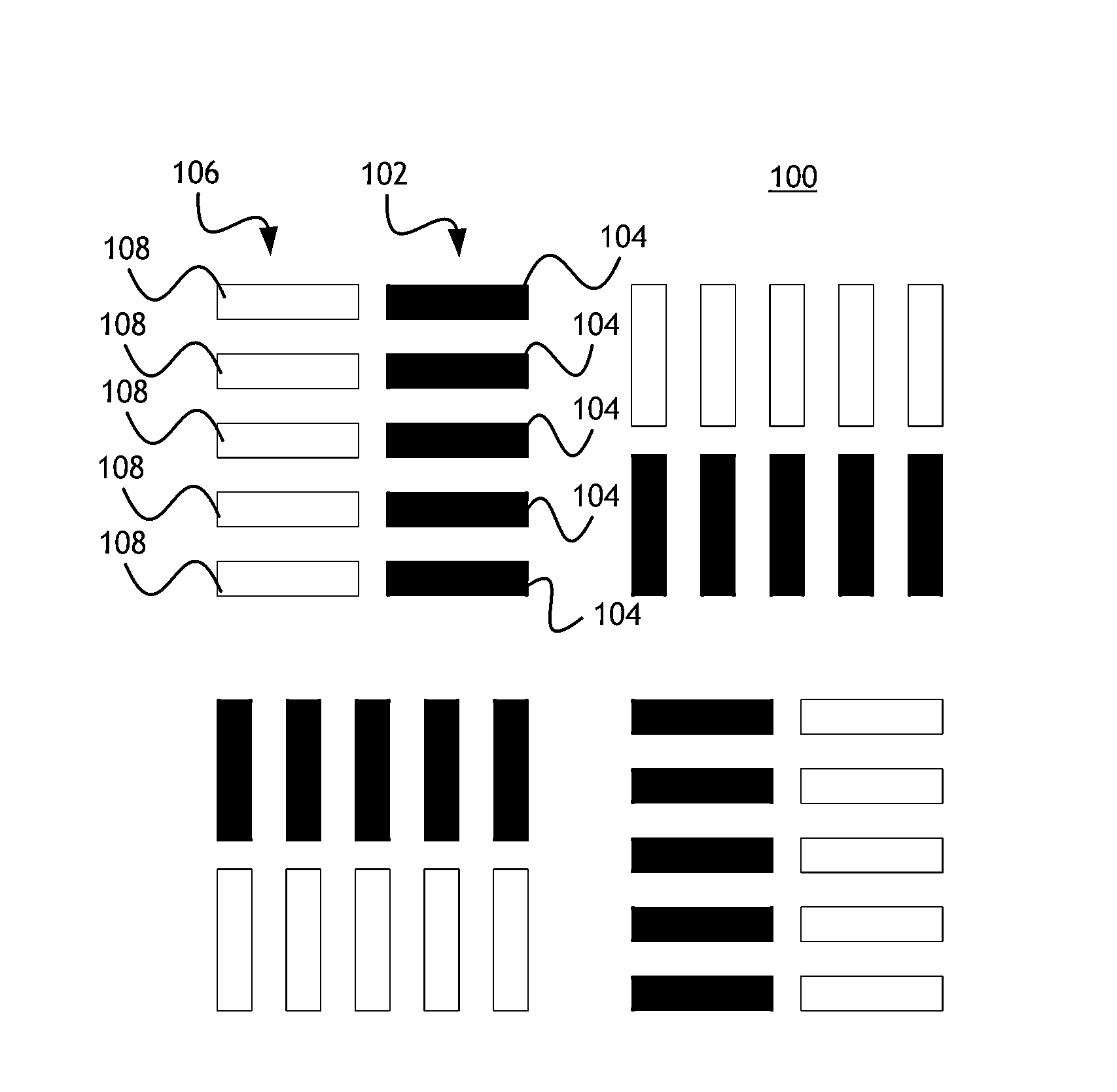
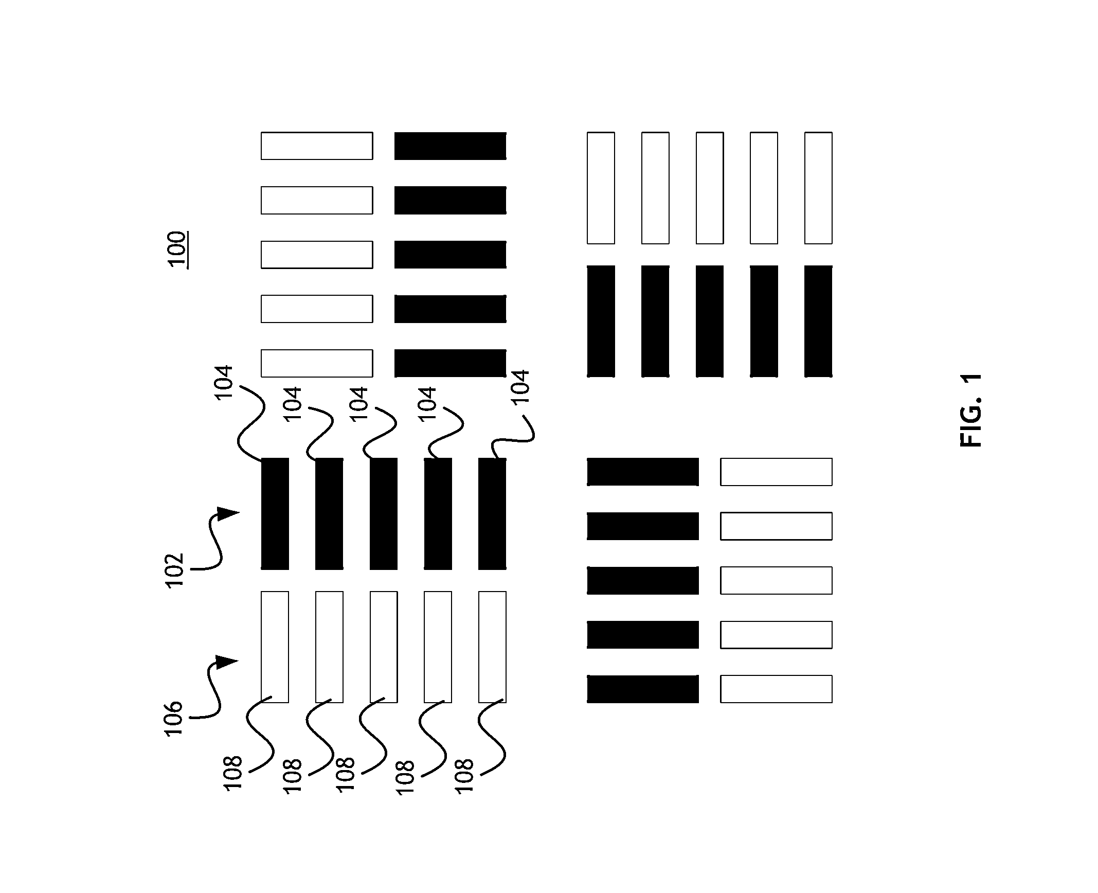
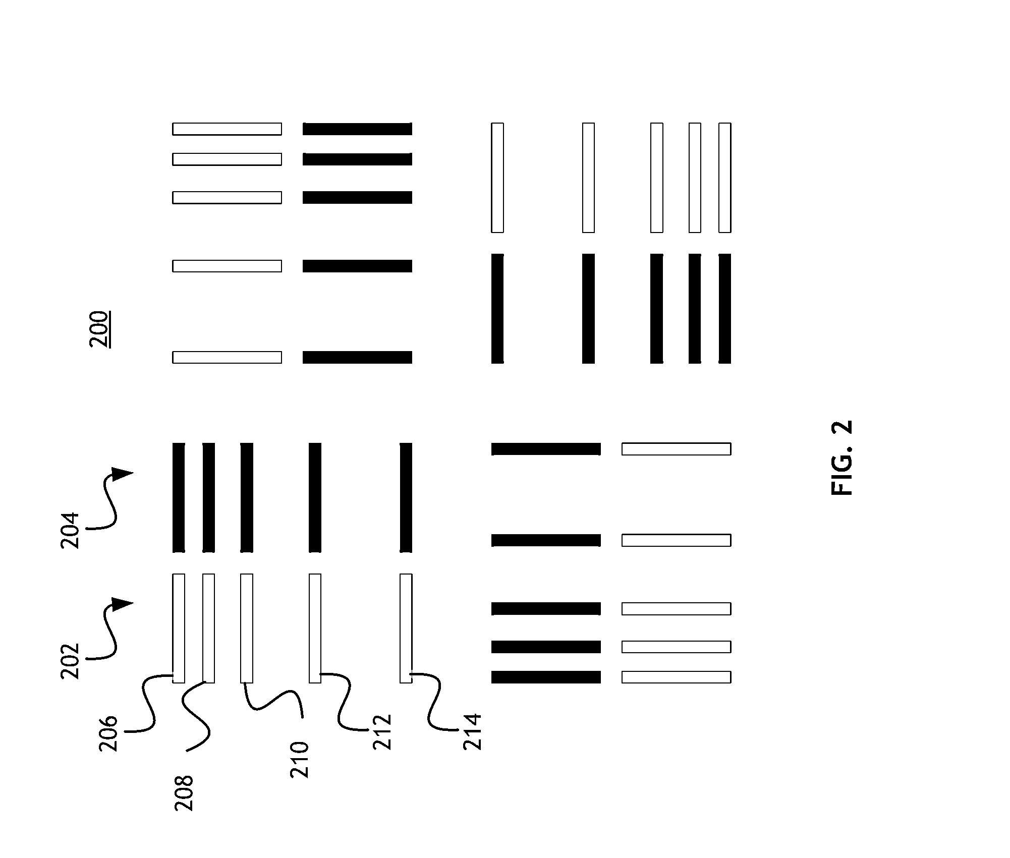
[0037]Referring generally to FIG. 2 through FIG. 7, an overlay target suitable for imaging based overlay metrology is described in accordance with the present disclosure. In a general sense, the overlay targets of the present invention may be used to determine overlay error between two successive process layers of a semiconductor wafer. For example, an overlay target may be utilized to measure the alignment of a first semiconductor layer with respect to a second semiconductor layer, where the second layer and the first layer are disposed succ...


PUM


Abstract

An overlay target for use in imaging based metrology is disclosed. The overlay target includes a plurality of target structures including three or more target structures, each target structure including a set of two or more pattern elements, wherein the target structures are configured to provide metrology information pertaining to different pitches, different coverage ratios, and linearity. Pattern elements may be separated from adjacent pattern elements by non-uniform distance; pattern elements may have non-uniform width; or pattern elements may be designed to demonstrate a specific offset as compared to pattern elements in a different layer.

Description

PRIORITY[0001]The present application claims the benefit under 35 U.S.C. §119(e) of U.S. Provisional Application Ser. No. 61 / 554,104, filed Nov. 1, 2011, which is incorporated herein by reference.FIELD OF THE INVENTION[0002]The present invention is directed generally toward overlay targets for semiconductor metrology, and more particularly toward overlay targets in semiconductors utilizing multiple pitches.BACKGROUND OF THE INVENTION[0003]Fabricating semiconductor devices such as logic and memory devices typically includes processing a substrate such as a semiconductor wafer using a large number of semiconductor fabrication processes to form various features and multiple levels of the semiconductor devices. For example, lithography is a semiconductor fabrication process that involves transferring a pattern from a reticle to a resist arranged on a semiconductor wafer. Additional examples of semiconductor fabrication processes include, but are not limited to, chemical-mechanical polis...

Claims


Application Information

Patent Timeline
Patent Type & Authority Applications(United States)
IPC IPC(8): G01B11/00H01L23/544
CPCG03F7/70683G03F7/70633
Inventor CHOI, DONGSUBTIEN, DAVID
Owner KLA CORP
Why Eureka
Try Eureka