Light Emitting Device
- Summary
- Abstract
- Description
- Claims
- Application Information
AI Technical Summary
Benefits of technology
Problems solved by technology
Method used
Image

Examples
embodiment 1
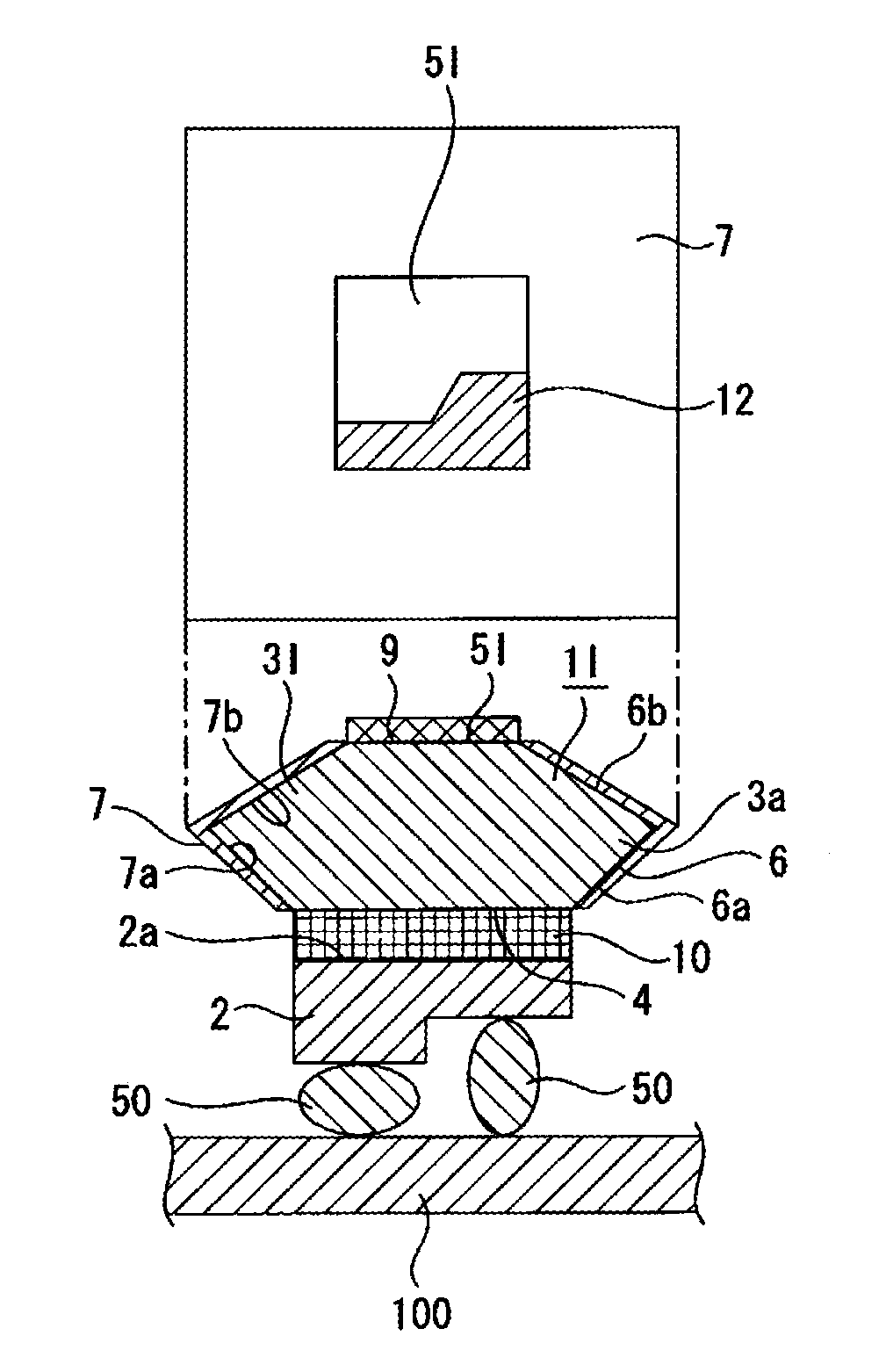
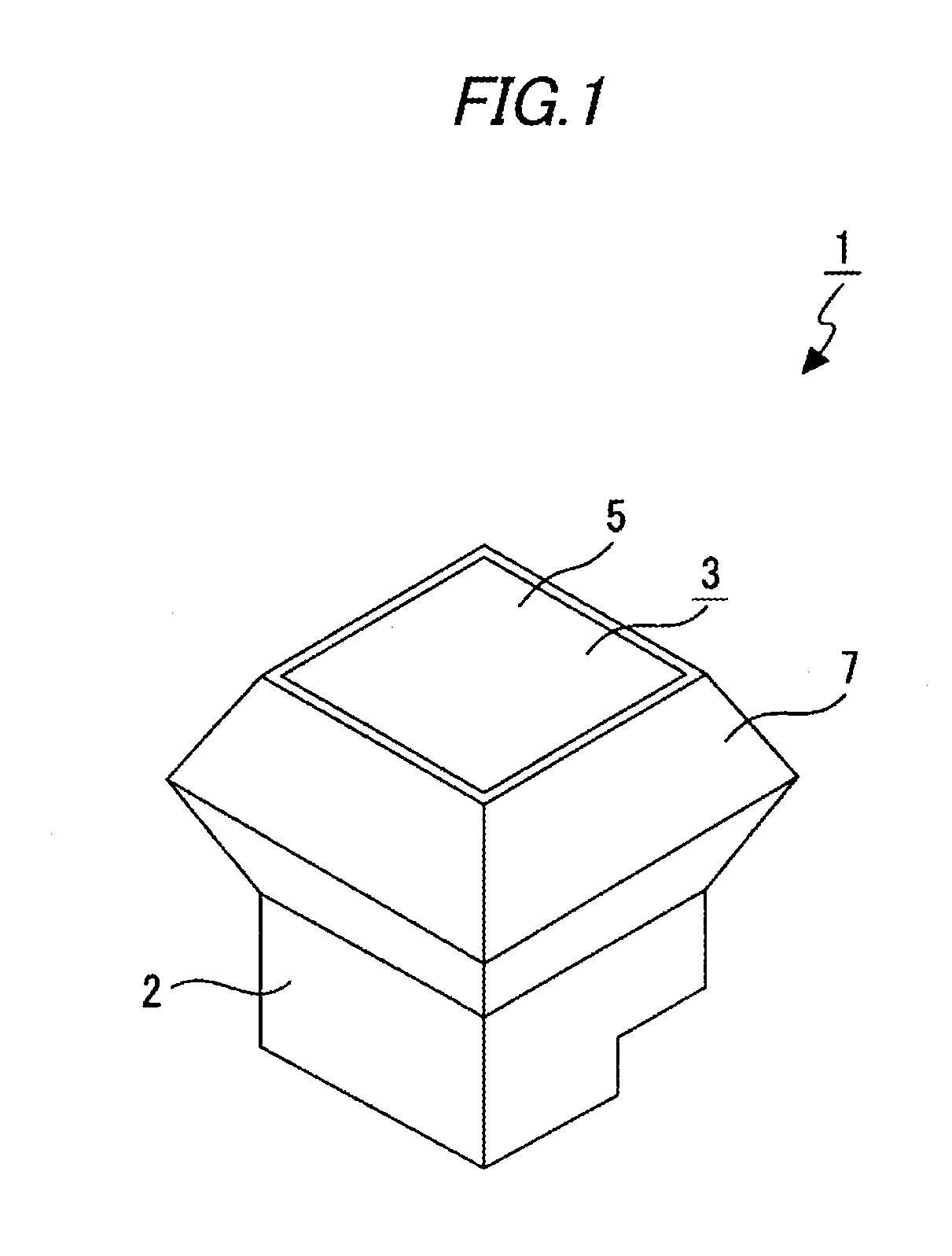
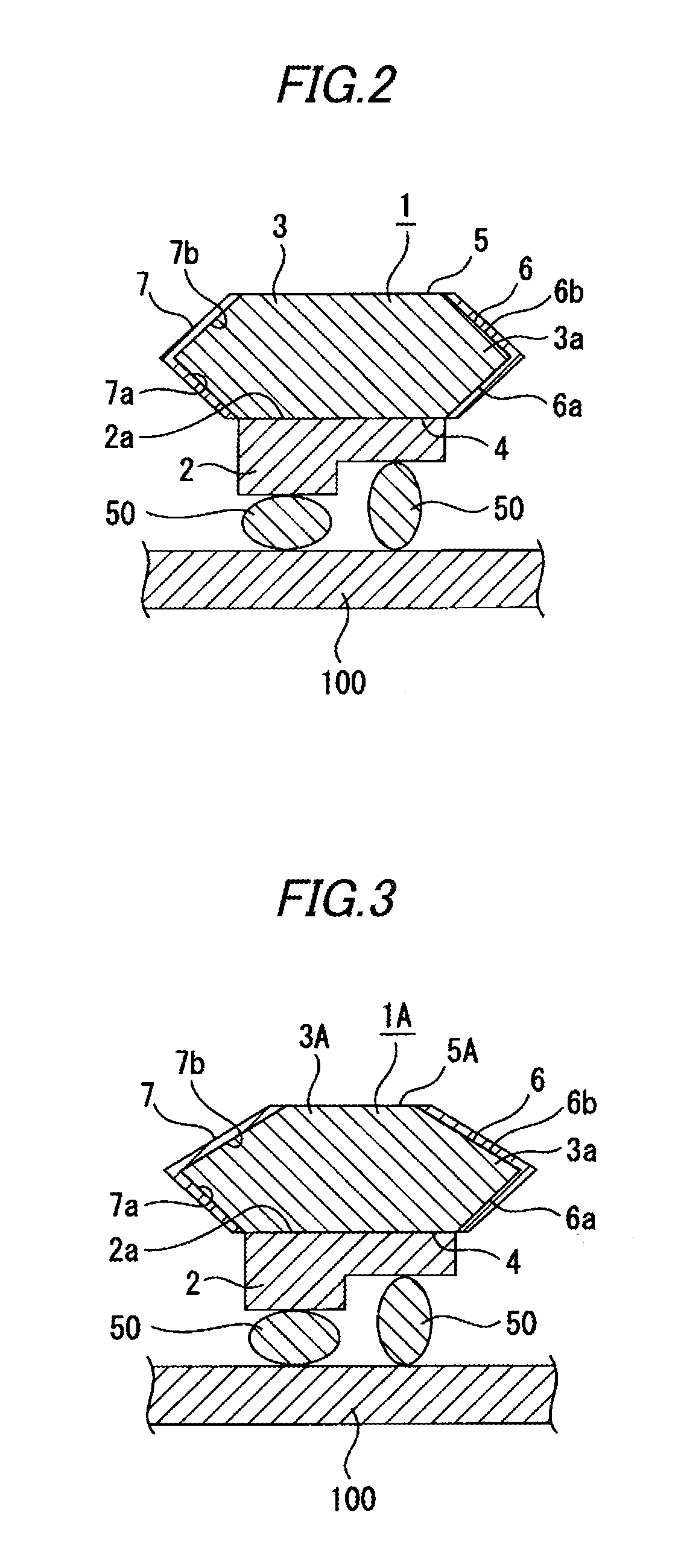
[0043]The light emitting device 1 according to embodiment 1 includes a semiconductor light emitting element 2 and a wavelength conversion layer 3 that is arranged on the semiconductor light emitting element 2 (refer to FIGS. 1 and 2).
[0044]In the light emitting device 1, the semiconductor light emitting element 2 is connected to a wiring pattern (not illustrated) of a substrate 100, for example, through bumps 50 and 50 by flip-chip mounting. Further, the semiconductor light emitting element 2 may be mounted on the substrate 100 by various mounting methods such as face up mounting.
[0045]The base material of the substrate 100 is formed of various materials, such as aluminum nitride, alumina, silicon, mullite, and copper, and the wiring pattern is connected to a feeding circuit (not illustrated). Accordingly, a driving current from the feeding circuit is supplied to the semiconductor light emitting element 2 through the wiring pattern of the substrate 100.
[0046]As the semiconductor lig...
embodiment 2
[0059]A light emitting device 1A according to embodiment 2 has a semiconductor light emitting element 2 and a wavelength conversion layer 3A that is arranged on the semiconductor light emitting element 2 (refer to FIG. 3).
[0060]The upper surface of the wavelength conversion layer 3A is formed as an output surface 5A, and the area of the output surface 5A is set to be smaller than the area of the input surface 4. The area of the output surface 5A is, for example, about 80% of the area of the input surface 4.
[0061]In the light emitting device 1A, since the area of the output surface 5A is smaller than the area of the input surface 4, the density of the light exited from the output surface 5A can be increased.
embodiment 3
[0062]A light emitting device 1B according to embodiment 3 has a semiconductor light emitting element 2 and a wavelength conversion layer 3B that is arranged on the semiconductor light emitting element 2 (refer to FIG. 4).
[0063]The upper surface of the wavelength conversion layer 3B is formed as an output surface 5B, and a minute concavo-convex shape 8 is formed on the output surface 5B. The concavo-convex portion 8 functions as a reflection suppression portion suppressing that the light incident to the wavelength conversion layer 3B through the input surface 4 is totally reflected by the output surface 5B.
[0064]In the light emitting device 1B, since the concavo-convex shape 8 is formed on the output surface 5B, it is suppressed that the light incident to the wavelength conversion layer 3B through the input surface 4 is totally reflected by the output surface 5B, and thus the light emitting efficiency can be improved.
PUM
 Abstract
Description
Claims
Application Information
 - R&D
- Intellectual Property
- Life Sciences
- Materials
- Tech Scout
- Unparalleled Data Quality
- Higher Quality Content
- 60% Fewer Hallucinations
Browse by: Latest US Patents, China's latest patents, Technical Efficacy Thesaurus, Application Domain, Technology Topic, Popular Technical Reports.
© 2025 PatSnap. All rights reserved.Legal|Privacy policy|Modern Slavery Act Transparency Statement|Sitemap|About US| Contact US: help@patsnap.com