

Method of manufacturing a wiring substrate for a display panel
- Summary
- Abstract
- Description
- Claims
- Application Information
AI Technical Summary
Benefits of technology
Problems solved by technology
Method used
Image

Examples
embodiment 1
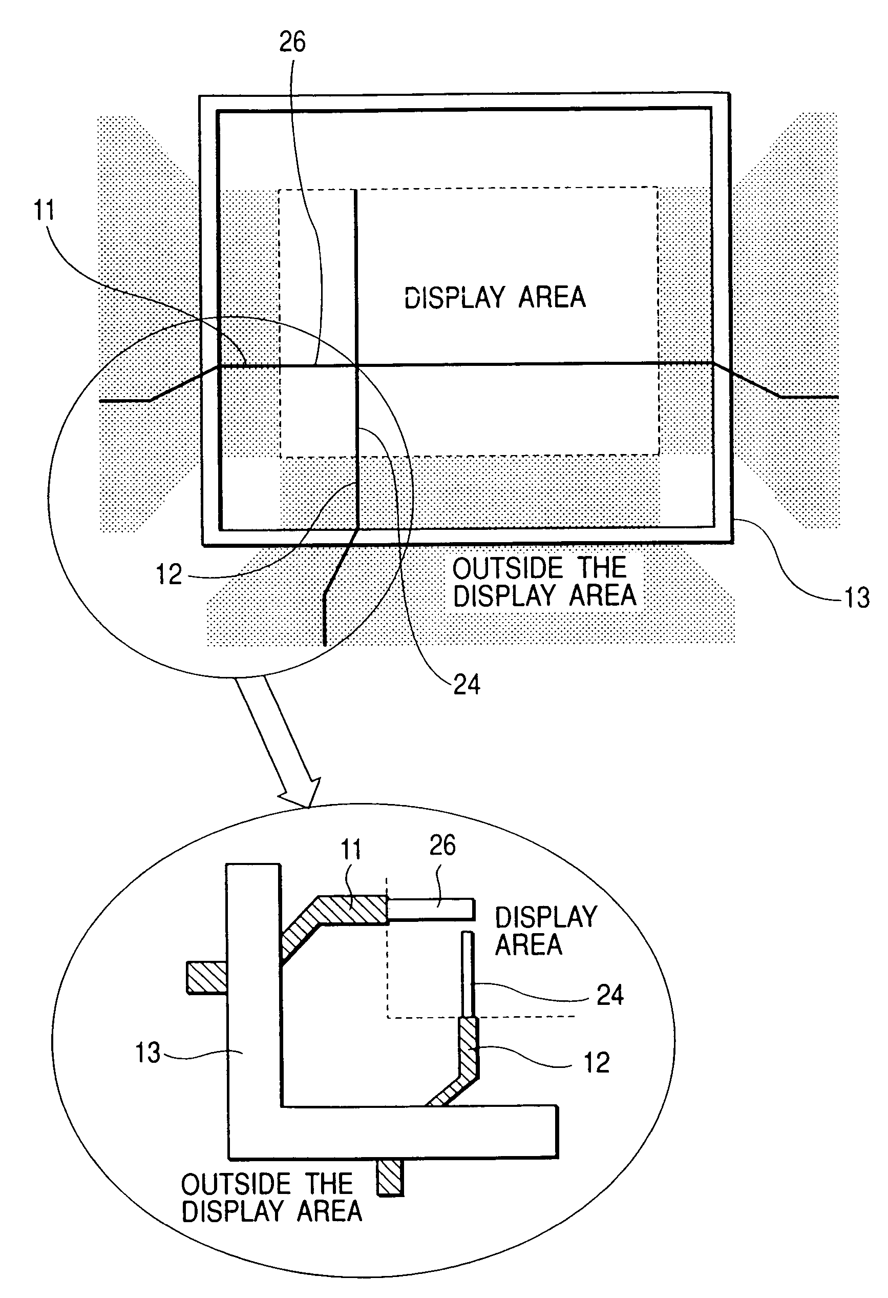
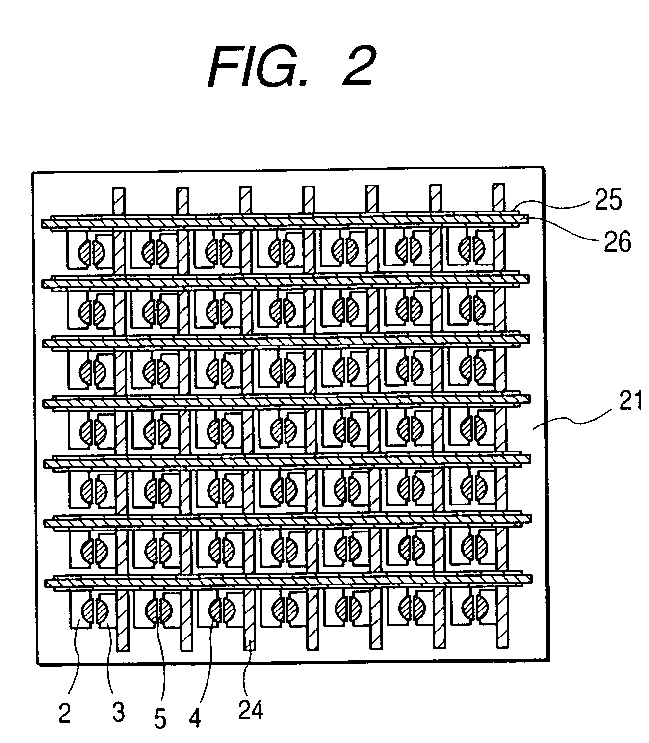
[0099]The present embodiment is an example where an electron source plate is formed by connecting multiple surface conduction electron-emitting devices to wirings in a matrix as illustrated in FIG. 2. In FIG. 2, reference numeral 21 denotes a substrate, 2 and 3 denote device electrodes, 4 denotes a conductive film (device film), 5 denotes an electron-emitting region, 24 denotes Y direction wirings (lower wirings), 25 denotes an insulating layer, and 26 denotes X direction wirings (upper wirings).
[0100]It is to be noted that FIG. 2 only illustrates the inside of the display area of the electron source plate. In an electron source plate actually manufactured, as illustrated in FIG. 1, the Y direction wirings 24 formed in the display area are connected to the Y direction drawn out wirings 12 outside the display area, and similarly, the X direction wirings 26 are connected to the X direction drawn out wirings 11. The X direction wirings 26 act as scanning electrodes after they are forme...
embodiment 2
[0136]In the present embodiment, both of X and Y direction drawn out wirings outside a display area are formed simultaneously with forming Y direction wirings in the display area. Both of the X and Y direction drawn out wirings are further coated with acrylic resin and, simultaneously, baking is carried out. Except this, an electron source plate is formed in a similar way as in the case of Embodiment 1. Only the wiring formation part is described in the following.
(Formation of Y Direction Wiring)
[0137]The Y direction wirings (lower wirings) 24 are formed by photolithography using a photo paste material so as to be in contact with and so as to connect the device electrodes 3 of the device electrodes 2 and 3 in a pattern as lines. Ag photo paste ink DC-206 (manufactured by Dupont) is used as the material. After screen printing and drying the material, exposure and development are carried out in a predetermined pattern. After that, baking is carried out at the temperature of about 480°...
embodiment 3
[0144]In the present embodiment, X and Y direction drawn out wirings outside a display area as first wirings are formed by photolithography using a photo paste. Further, as second wirings, second layer drawn out wirings are formed by screen printing using paste ink for printing which is not photolithographic paste on the X and Y direction drawn out wirings outside the display area (first wirings). Except this, an electron source plate is formed in a similar way as in the case of Embodiment 1. Only the wiring formation part is described in the following.
(Formation of Y Direction Wiring)
[0145]The Y direction wirings (lower wirings) 24 are formed by photolithography using a photo paste material so as to be in contact with and so as to connect the device electrodes 3 of the device electrodes 2 and 3 in a pattern as lines. Ag photo paste ink DC-206 (manufactured by Dupont) is used as the material. After screen printing and drying the material, exposure and development are carried out in ...
PUM
 Abstract
Description
Claims
Application Information