Semiconductive nanowire solid state optical device and control method thereof

a technology of semi-conductive nanowires and optical devices, which is applied in the direction of semi-conductive devices, electrical devices, nanotechnology, etc., can solve the problems of human beings' toughest challenges

Inactive Publication Date: 2013-05-23
NAT APPLIED RES LAB
View PDF0 Cites 4 Cited by
  • Summary
  • Abstract
  • Description
  • Claims
  • Application Information

AI Technical Summary

Benefits of technology

[0017]The present invention also provides a control method of a semiconductor nanowire solid state optical device and the semiconductor nanowire solid state optical device comprises a nanowire, an electrical circuit and a mechanical micro device, which is conjuncted with the nanowire. The control method comprises applying an external force to the nanowire by the mechanical micro device to form highest occupied molecular orbital and lowest unoccupied molecular orbital in the nanowire.
[0018]According to the present invention, the nanowire can be employed as an electroluminescence device. The control method of the present invention further comprises a step of applying electrical power to the nanowire for causing the nanowire illuminate.
[0019]According to the present invention, the nanowire can be employed as a photovoltaic device. The control method of the present invention further comprises a step of a step of shining the nanowire with light to cause the nanowire to generate an electric current.
[0020]The semiconductor nanowire solid state optical device and the control method of present invention does not require doping or fabrication of heterostructure to form a semiconductor optical device with a PN interface which is necessary in prior arts. The present invention merely applies an external force, such as twisting the nanowire and the nanowire can become a semiconductor with a PN interface. The mechanical micro device is employed as a switch of the semiconductor solid state optical device according to the present invention. Once the external force applied to the nanowire is erased, the solid state optical device of the present invention, which is employed as a photovoltaic device or an electroluminescence device stop its function.

Problems solved by technology

The harshest challenge of human beings today is to think through a way of eternal survive in the future.

Method used


Image

  • Semiconductive nanowire solid state optical device and control method thereof
  • Semiconductive nanowire solid state optical device and control method thereof
  • Semiconductive nanowire solid state optical device and control method thereof

Examples


first embodiment

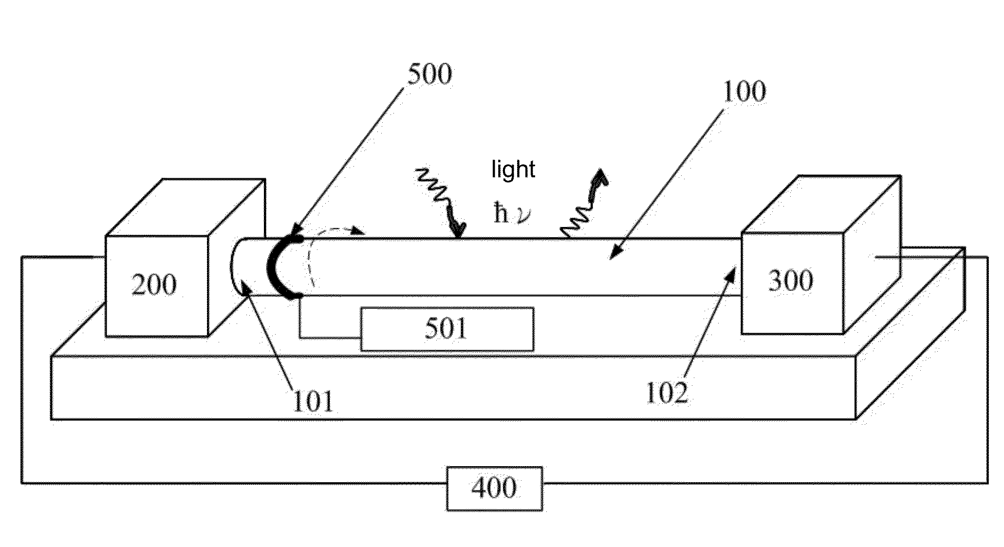
[0033]Please refer to FIG. 3, FIG. 5A to FIG. 5D, which show front view and sectional view relationship diagrams between the twist angle of the nanowire 100 according to the present invention and the highest occupied molecular orbital (HOMO), the lowest unoccupied molecular orbital (LUMO) by simulation software analysis. In this embodiment, the direction of the nano-crystal structure in the nanowire 100 is . The diameter of the nanowire 100 is 1.5 nm. The nanowire 100 is a silicon nanowire which is fabricated by a single material and comprises silicon nano-crystal structures. However, the present invention is not limited thereto. The material of the nanowire 100 can selected from group 2 elements, triels, tetrels and pentels.

[0034]FIG. 5A and FIG. 5B show a front view diagram of the nanowire 100. FIG. 5C and FIG. 5D show a sectional view diagram of the nanowire 100. FIG. 5A and FIG. 5C show the electron and electron hole distributions in the nanowire 100 when the mechanical micro de...

second embodiment

[0035]Please refer to FIG. 3, FIG. 6A to FIG. 6C, which show front view and sectional view relationship diagrams between the twist angle of the nanowire 100 according to the present invention and the highest occupied molecular orbital (HOMO), the lowest unoccupied molecular orbital (LUMO) by simulation software analysis. In this embodiment, the direction of the nano-crystal structure in the nanowire 100 is . The diameter of the nanowire 100 is 1.5 nm. The nanowire 100 is a silicon nanowire which is fabricated by a single material and comprises silicon nano-crystal structures. However, the present invention is not limited thereto. The material of the nanowire 100 can selected from group 2 elements, triels, tetrels and pentels.

[0036]FIG. 6A and FIG. 6B show a front view diagram of the nanowire 100. FIG. 6C shows a sectional view diagram of the nanowire 100. FIG. 6A and FIG. 6C show the electron and electron hole distributions in the nanowire 100 when the mechanical micro device 500 ap...

third embodiment

[0037]Please refer to FIG. 3, FIG. 7A to FIG. 7C, which show front view and sectional view relationship diagrams between the twist angle of the nanowire 100 according to the present invention and the highest occupied molecular orbital (HOMO), the lowest unoccupied molecular orbital (LUMO) by simulation software analysis. In this embodiment, the direction of the nano-crystal structure in the nanowire 100 is . The diameter of the nanowire 100 is 2.2 nm. The nanowire 100 is a silicon nanowire which is fabricated by a single material and comprises silicon nano-crystal structures. However, the present invention is not limited thereto. The material of the nanowire 100 can selected from group 2 elements, triels, tetrels and pentels.

[0038]FIG. 7A and FIG. 7B show a front view diagram of the nanowire 100. FIG. 7C shows a sectional view diagram of the nanowire 100. FIG. 7A shows the electron and electron hole distributions in the nanowire 100 when the mechanical micro device 500 applies the e...


PUM


Abstract

Disclosed are a semiconductor nanowire solid state optical device and a control method thereof. The device comprises a nanowire, a first electrode, a second electrode, an electrical circuit and a mechanical micro device. The nanowire has a first end and a second end. The first electrode is coupled to the first end. The second electrode is coupled to the second end. The electrical circuit is coupled to the first electrode and the second electrode. The mechanical micro device is conjuncted with the nanowire for applying an external force to the nanowire to form highest occupied molecular orbital (HOMO) and lowest unoccupied molecular orbital (LUMO) in the nanowire. The HOMO and LUMO are employed as an n-type semiconductor and a p-type semiconductor, respectively. The nanowire is a semiconductor when an external force is applied thereto.

Description

BACKGROUND OF THE INVENTION[0001]1. Field of the Invention[0002]The present invention generally relates to a semiconductor nanowire solid state optical device, and more particularly to a semiconductor nanowire solid state optical device for being an electroluminescence device or a photovoltaic device and control method thereof.[0003]2. Description of Prior Art[0004]The harshest challenge of human beings today is to think through a way of eternal survive in the future. Kinds of topics, such as rapid global population growth, global warming, climate change, lack of basic survive resource and serious pollution of the earth environment and etc. are all severe predicaments that the human beings have to face and deal with. As regarding the topics of deficient energy, the ascendant solar energy and LED industries may be considered as the solutions of solving the deficient energy for the human beings in the future and therefore become important and major possibilities. Today, products of re...

Claims


Application Information

Patent Timeline
Patent Type & Authority Applications(United States)
IPC IPC(8): H01L33/06H01L31/0352B82Y20/00
CPCH01L33/18B82Y20/00H01L31/08H01L31/035227
Inventor SHIH, YU-CHINGLEE, JIUNN-HORNGCHEN, CHIA-CHINLIN, CHI-FENGFANG, YU-BINLEE, MING-HSIAOKAN, HENG-CHUAN
Owner NAT APPLIED RES LAB
Why Eureka
Try Eureka