Radar component package and method for manufacturing the same

a technology of radar components and components, applied in the direction of instruments, structural forms of radiating elements, using reradiation, etc., can solve the problems of a large amount of components, a large amount of losses, so as to reduce the thickness of the package and reduce the loss

Active Publication Date: 2022-05-31
NAT CENT FOR ADVANCED PACKAGING
View PDF10 Cites 0 Cited by
  • Summary
  • Abstract
  • Description
  • Claims
  • Application Information

AI Technical Summary

Benefits of technology

[0005]It is an object of the invention to provide a millimeter wave radar component package and a method for manufacturing such millimeter wave radar component package, which may reduce losses and substantially decrease thickness of the package.
[0021]The millimeter wave radar component package according to the invention has at least the following advantages: (1) the millimeter wave radar component package according to the invention has a relatively low loss, because the chips of the package are arranged in flip chip manner, so that the lengths of wires are reduced, thereby decreasing the loss; (2) in the present invention, the thickness of the entire package may be reduced by embedding the chips, the antenna and the conductive lines into respective insulators of the box body; (3) in the present invention, because the chips, the antenna and the conductive lines are embedded into respective insulators of the box body and the conductive lines are exposed (i.e. Fan Out Package), the substrate may be omitted, thereby further reducing the thickness of the package.
[0026]By means of this embodiment, the millimeter wave radar chip and the related functional chips may be integrated in the same package, so that the integration degree can be enhanced.
[0031]In yet another embodiment of the invention, it is provided that, the metal barrier layer comprises TiCu or TiWCu, and has a thickness of 1-10 μm. In the present invention, the metal barrier layer serves as etching stopping layer when etching the second insulator or opening the channel, and furthermore, it realizes electrical contact between the pads of the chips and the conductive lines. By means of this embodiment, a metal barrier layer with good etching stopping function and electrically conducting function may be realized.
[0033]In another embodiment of the invention, it is provided that, the metal layer comprises titanium, copper, nickel, tungsten, silver, gold or alloys thereof. By means of this embodiment, a good reception and transmission of the antenna signal may be realized.
[0044]The method according to the invention also has the advantages the millimeter wave radar component package according to the invention, i.e. reducing loss and thickness of the package.

Problems solved by technology

However, insufficiencies of this encapsulated millimeter wave radar transceiving component lie in that the chips are arranged by wire bonding, which leads not only to too long wire and higher losses, but also to a higher thickness of the component, because a certain height is reserved in the box body for the wire of wire bonding.
Furthermore, the manufacturing of this encapsulated millimeter wave radar transceiving component adopts a traditional packaging process including steps of mounting chips, bonding wires, and fabricating substrates, so that the thicknesses of substrates and chips hinder a further reduction of the thickness of the component.

Method used


Image

  • Radar component package and method for manufacturing the same
  • Radar component package and method for manufacturing the same
  • Radar component package and method for manufacturing the same

Examples


Embodiment Construction

[0054]It should be pointed out that, components in the drawings may be shown in an exaggerated form for the purpose of illustration, instead of being true to scale. In the drawings, same or functionally same components are provided with same reference numerals.

[0055]Unless otherwise specified, in the present application, the articles “a” and “an” do not exclude scenarios with multiple elements.

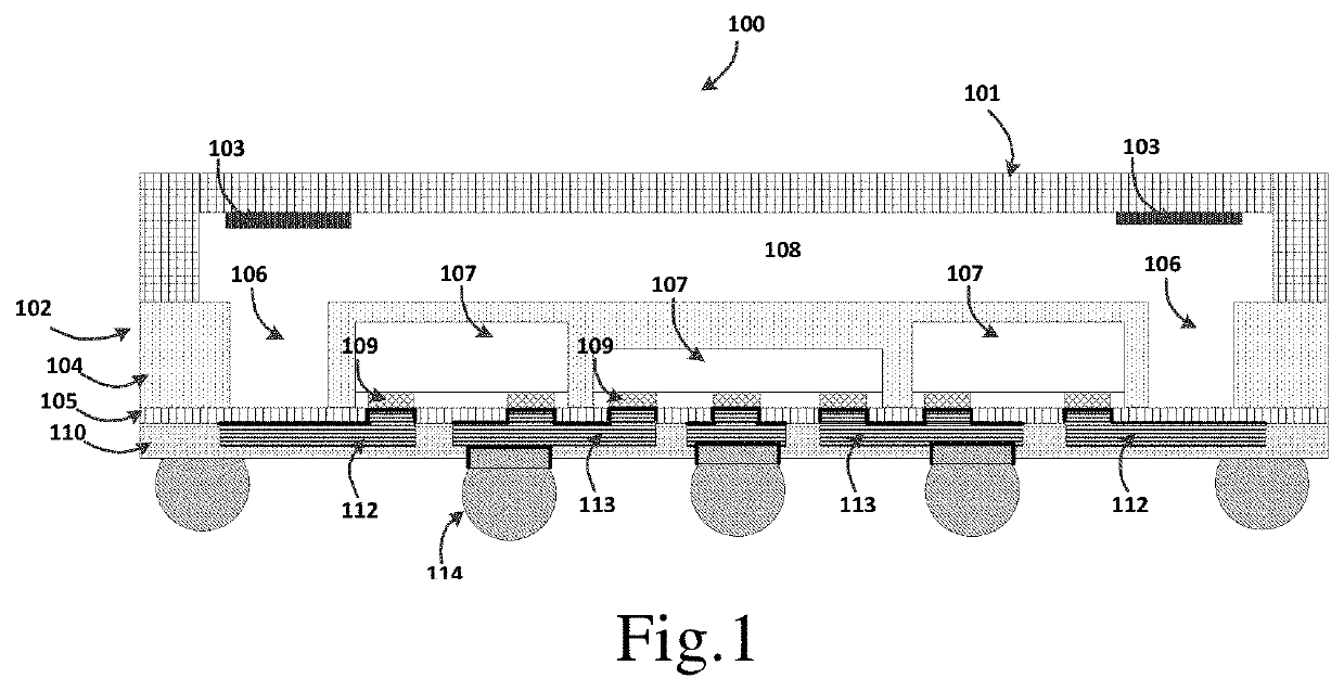
[0056]FIG. 1 illustrates a schematic view of the millimeter wave radar component package 100 according to the invention.

[0057]As shown in FIG. 1, the millimeter wave radar component package 100 according to the invention includes a box cover 101 and a box body 102.

[0058]The box cover 101 may be made of a low dielectric constant material, for example, Polytetrafluoroethylene. On an inner surface of the box cover 101, a metal layer 103 is arranged which is made of, for example, titanium, copper, nickel, tungsten, silver, gold or alloys thereof. The reception and transmission of signal by antenna...


PUM


Abstract

The present invention relates to a millimeter wave radar component package, comprising: a box cover, having a metal layer arranged on inner surface of the box cover, the metal layer facing a channel of a box body, wherein a cavity is formed between the box cover and the box body; and the box body, comprising: a first insulator, connected with the box cover, wherein in the first insulator a channel is opened, and one end of the channel corresponds with the position of antenna and the other end is connected with the cavity; one or more chips, arranged on a second insulator in a flip manner and covered by the first insulator; the second insulator, arranged between the first insulator and a third insulator; the third insulator; and the antenna and conductive lines, arranged in the third insulator and connected with pads of the one or more chips through the second insulator, wherein the conductive lines are exposed from the third insulator for electrical contact. The present invention further relates to a method for manufacturing the package.

Description

CROSS REFERENCE TO RELATED APPLICATIONS[0001]This application is a national stage application of International Application No. PCT / CN2017 / 113113, filed on Nov. 27, 2017, which claims priorities to Chinese Patent Application Nos. 201710709853.6, filed on Aug. 18, 2017, and 201710717924.7, filed on Aug. 18, 2017, all of which are hereby incorporated by reference in their entireties.TECHNICAL FIELD[0002]The invention relates generally to the field of semiconductor manufacture, and specifically, to a millimeter wave radar component package and a method for manufacturing such millimeter wave radar component package.BACKGROUND[0003]As the consumption products are increasingly diversified in their functions, there is a need for wireless detection (for example detecting moving object and its speed) in many domains such as automobile, rotor, smart phone and etc., therefore, the application of the millimeter wave radar component is increased day by day. However, applications in many domains s...

Claims


Application Information

Patent Timeline
Patent Type & Authority Patents(United States)
IPC IPC(8): G01S7/03H01L21/48H01L21/54H01L21/56H01L23/053H01L23/20H01L23/31H01L23/538H01L23/66H01L23/00H01Q1/22H01Q23/00G01S7/02
CPCG01S7/032H01L21/4817H01L21/4853H01L21/4857H01L21/54H01L21/565H01L21/568H01L23/053H01L23/20H01L23/3128H01L23/5383H01L23/5386H01L23/5389H01L23/66H01L24/19H01L24/20H01Q1/2283H01Q23/00G01S7/028H01L2223/6677H01L2224/214H01L2224/24137H01L2224/96H01L2224/04105H01L2224/12105H01Q1/38H01Q1/42H01Q9/0414H01L23/055H01L21/56G01S13/931H01L2924/3025H01L2924/1815H01L25/0655H01L23/552H01L25/50H01L23/49816H01L23/49822H01L21/4846
Inventor ZHANG, WENQICHEN, FENG
Owner NAT CENT FOR ADVANCED PACKAGING
Why Eureka
Try Eureka