Organic electroluminescence device

Inactive Publication Date: 2013-05-23
TOPPAN PRINTING CO LTD
View PDF2 Cites 4 Cited by
  • Summary
  • Abstract
  • Description
  • Claims
  • Application Information

AI Technical Summary

Benefits of technology

[0015]According to the invention, two or more kinds of polymer materials having different carrier mobilities are mixed, and the combination and the mixing ratio of the materials to be mixed are controlled, whereby new functions may be imparted co

Problems solved by technology

Accordingly, for emitting light with an increased luminance at a reduced operation voltage, it is necessar

Method used


Image

  • Organic electroluminescence device
  • Organic electroluminescence device
  • Organic electroluminescence device

Examples


Example

EXAMPLE

[0086]Examples of the organic thin film electroluminescence display equipment of the invention will be described below, but the invention is not limited to the examples.

Example

Example 1

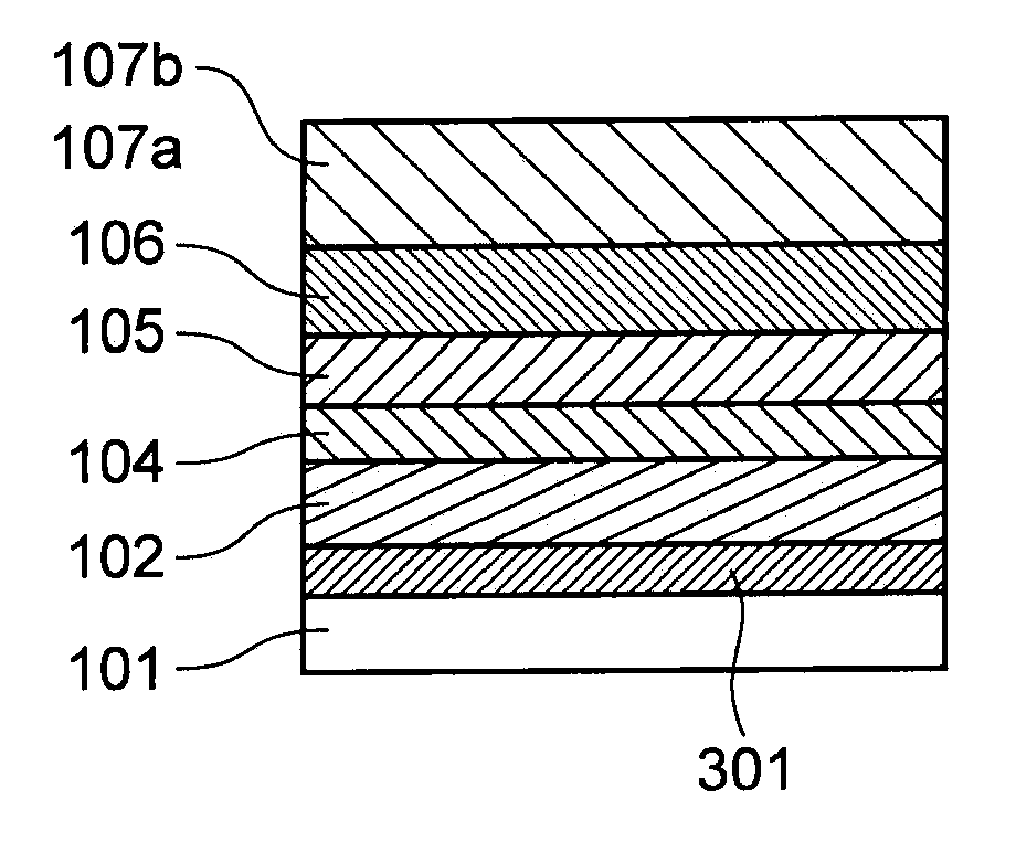
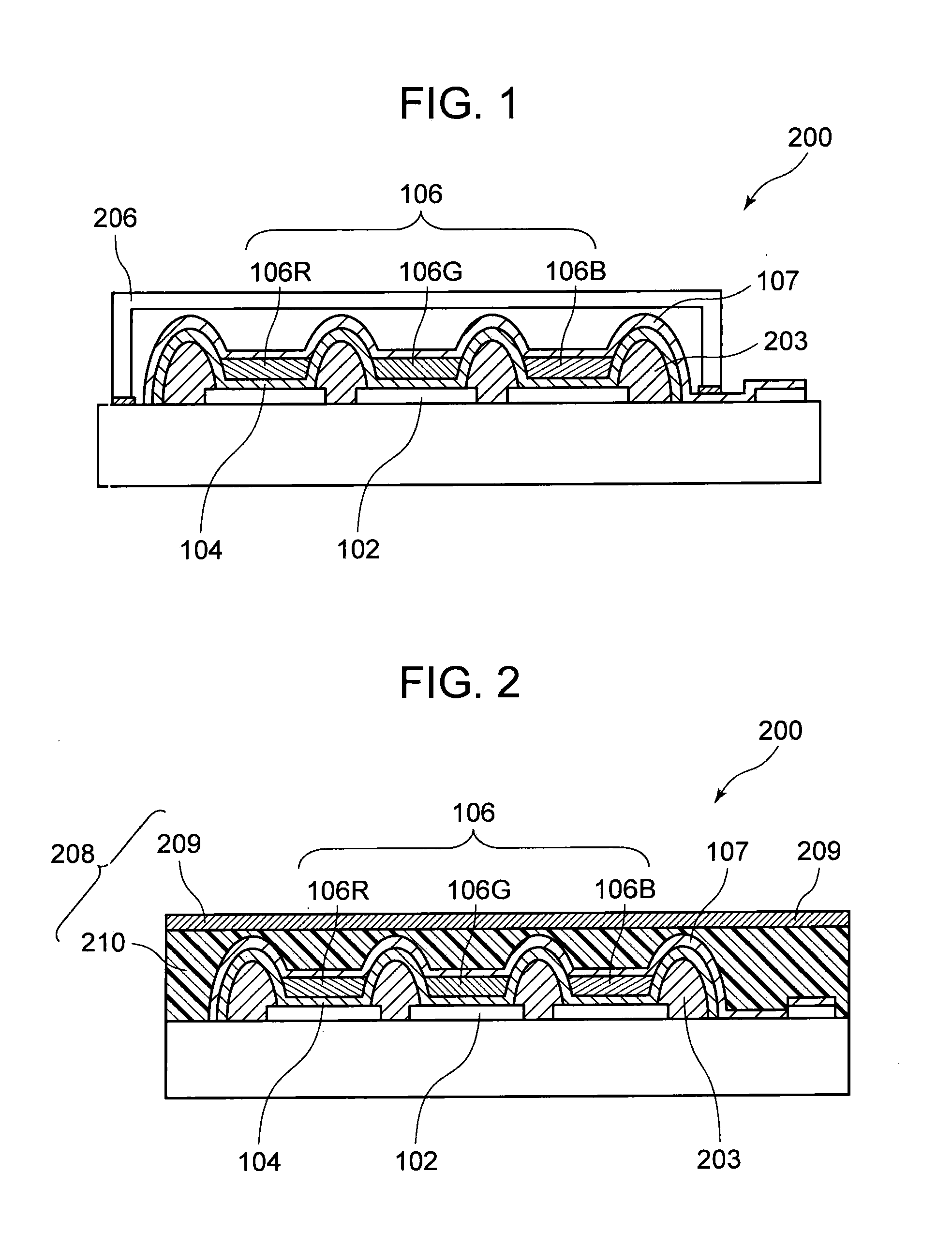
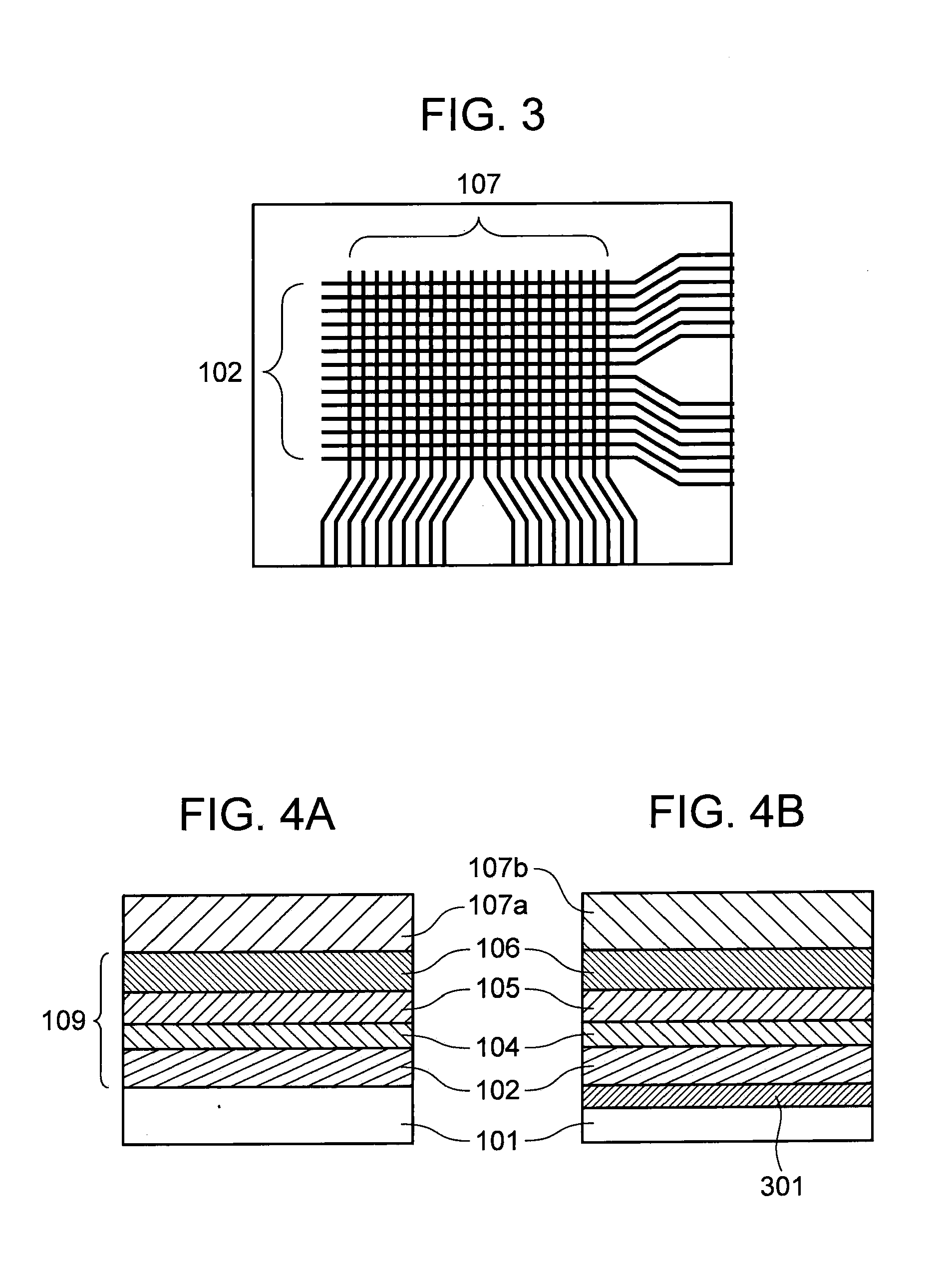
[0087]On a glass substrate having a diagonal length of 1.8 inch as a light permeable substrate, an ITO (indium tin oxide) thin film was formed by a sputtering method, and the ITO film was patterned by a photolithography method and an etching method with an acid solution, thereby forming pixel electrodes. The line pattern of the pixel electrodes was a line width of 136 μm and a space of 30 μm, in which 192 lines were formed within a square of approximately 32 mm.

[0088]A partition wall was then formed in the following manner. A positive photosensitive polyimide (Photoneece DL-1000, produced by Toray Industries, Inc.) was spin-coated over the entire surface of the glass substrate having the pixel electrodes formed thereon. The condition of spin coating was rotation at 150 rpm for 5 seconds and then rotation at 500 rpm for 20 seconds per one time of coating, and the height of the partition wall was 1.5 μm. The photosensitive material coated on the entire surface was subjected t...

Example

Example 2

[0096]In Example 2, the organic light emitting ink A and the organic light emitting ink B were mixed at a weight ratio of 80 / 20 to prepare a mixed ink II. A light emitting layer was printed by a relief printing method immediately on the pixel electrodes surrounded by the partition wall according to the line pattern thereof. The thickness of the light emitting layer after printing and drying was 100 nm. The other conditions were the same as in Example 1. On driving the resulting organic EL display panel, it exhibited a luminance of 600 cd / cm2 and a CIE chromaticity of x=0.31 and y=0.63 at a driving voltage of 7 V, and the service life at an initial luminance of 1,000 cd / m2 was 250 hours.


PUM

PropertyMeasurementUnit
Percent by massaaaaaaaaaa
Areaaaaaaaaaaa
Hole mobilityaaaaaaaaaa

Abstract

A display equipment 200 containing an organic EL device is constituted by containing a substrate 101 having thereon a first electrode 102 provided for respective pixels, a partition wall 203 partitioning the first electrode 102 among the pixels, a hole transporting layer 104 formed above the first electrode 102, a light emitting layer 106 formed on the hole transporting layer 104, a second electrode 107 formed to cover the entire surface of the light emitting layer 106, and a sealing member 208 in contact with the substrate 101 to cover the first electrode 102, the partition wall 203, a light emitting medium layer 109 containing the hole transporting layer 104 and the light emitting layer 106, and the second electrode 107.

Description

CROSS REFERENCE TO RELATED APPLICATION[0001]This application is a continuation of International Application No. PCT / JP2011 / 065351, filed on Jul. 5, 2011 the entire contents of which are incorporated herein by reference.TECHNICAL FIELD[0002]The present invention relates to an organic electroluminescence display equipment (which may be hereinafter referred to as an organic EL display equipment) containing arranged therein an organic electroluminescence device (which may be hereinafter referred to as an organic EL device) utilizing an organic electroluminescence phenomenon. More specifically, the invention relates to an organic electroluminescence display equipment that has a simple structure, has new functions imparted by a simple process to functional layers constituting the organic EL devices, and has a improved efficiency and a decreased operation voltage.BACKGROUND ART[0003]In an organic EL device, an electroconductive light emitter is applied with a voltage to recombine the injec...

Claims


Application Information

Patent Timeline
IPC IPC(8): H01L51/50
CPCH01L27/3283H01L51/0004H01L51/5036H01L51/5012H01L51/0035H10K59/173H10K71/13H10K85/111H10K50/125H10K50/11H01L2031/0344H10K85/10
Inventor MORIKAWA, NORIKOKITAZUME, EIICHI
Owner TOPPAN PRINTING CO LTD
Why Eureka
Try Eureka