Optical system and method for inspection of patterned samples

a technology of optical system and sample, applied in the field of optical inspection, can solve the problems of bf inspection reaching its limit, certain defects cannot be detected by traditional bf inspection systems, etc., and achieve the effect of increasing the collection region of scattered light, maximizing the effective collection region, and increasing the pitch siz

Inactive Publication Date: 2013-06-13
APPL MATERIALS ISRAEL LTD
View PDF3 Cites 12 Cited by
  • Summary
  • Abstract
  • Description
  • Claims
  • Application Information

AI Technical Summary

Benefits of technology

[0014]The present invention provides a novel optical inspection technique enabling optimal performance of a dark field inspection mode irrespective of the actual location of a light collection channel with respect to an illumination / specular reflection azimuth and elevation. To this end, the invention utilizes an appropriate arrangement of illumination and collection masks (masks' accommodation and patterns) to optimize light collection with desirably high resolution, i.e., enabling a sufficiently large collection region (for a given light collection channel) with a desirably small illumination spot. It should be noted that the mask (illumination and / or collection pattern) may have a static pattern or may be constituted by an electronic spatial coding in which case the pattern may be dynamic. In any case, the technique of the present invention provides for appropriately varying the mask pattern, e.g., by using a switching mechanism for replacing one mask by another having a different static pattern or for appropriately varying a code of the electronic unit (spatial light modulator).
[0015]It should be understood that a bright-field inspection mode is aimed at inspecting the pattern itself. In a bright-field mode, an imaging system collects light reflected from the sample including light components associated with diffraction orders (resulting from the periodicity of the pattern) providing information indicative of as many spatial details of the inspected pattern as possible by optical limitations of the system. On the other hand, a dark-field inspection mode utilizes collection of scattered light while blocking or significantly reducing collection of light reflected directly from the pattern on the sample.
[0016]As indicated above, dark-field inspection mode includes collection of light scattered from a possible defect. The defect is identified as a bright spot over dark background. The collection of scattered light can be done by orienting a light collection channel outside the azimuth and elevation of propagation of specular reflection from a sample, thus collecting substantially scattered light (signal) and also high order diffraction components (noise) having relatively low intensity. In other configurations, dark-field imaging techniques may utilize light collection with angular orientation of a collection channel passing through or in the vicinity of the orientation of specular reflection path. A collection mask can be utilized for blocking light components associated with diffraction orders and thus increase signal to noise ratio (SNR) and improving efficiency of the defect detection.
[0019]In the simplest case of “normal inspection mode”, where illumination and collection channels coincide, the apertures of the illumination mask are made in or aligned with at least some of the blocking regions of the light collection mask. In a generalized case, where illumination and collection channels may or may not coincide (oblique illumination), the illumination and collections masks are located at corresponding spectral planes with respect to the sample plane. It should be understood that these corresponding planes are typically Fourier planes with respect to the sample, or can be referred to as conjugate planes of one another (i.e., “pupil” and “image” planes and vice versa). In this case, an arrangement of apertures of the illumination mask and an arrangement of the blocking regions of the collection mask are selected to optimize (maximize) an effective collection region. Light passing through the illumination mask and returned from the pattern of the sample forms diffraction lobes each being an image of the illumination mask. Thus, by varying the shape of the diffraction lobes (i.e., by appropriately designing the illumination mask) the collection region of scattered light can be increased.
[0020]It should be understood that the technique of the present invention is especially useful for inspection of patterned samples having a certain asymmetry along two axes of the sample (different periodicities of the pattern along different axes). As will be explained below, a typical pitch size of the pattern along a certain axis (defined as an x- or y-axis along the surface of the sample) determines a distance between the centers of diffraction lobes along the same axis. When the typical pitch size of the pattern is different along the x- and y-axes, the arrangement of the diffraction lobes is different. Assuming a patterned sample having a substantially rectangular optical unit cell (reappearing pattern which spans the surface), having larger pitch size along the x-axis, the distances between the centers of the diffraction lobes along the x-axis will be smaller than those along the y-axis. The technique of the present invention may utilize the asymmetry of the pattern to optimize the collection region by appropriately shaping the illumination pupil, and thus the diffraction lobes, to stretch the diffraction lobes along one axis, while keeping them narrow along the other axis. More specifically, if the pattern has larger pitch size along the x-axis, the illumination pupil will be relatively wider along the x-axis and relatively narrow along the y-axis. Moreover, the use of multiple illumination apertures arranged with the same relation between their centers as that of the diffraction lobes pattern increases the amount of illumination reaching the patterned surface and thus increases the efficiency of the inspection. Utilizing an array of apertures may also provide for a smaller illumination spot on the sample. A smaller illumination spot increases accuracy and sensitivity of the inspection.

Problems solved by technology

When dealing with patterns having a pitch size (features) much smaller than the optical spot size on the wafer (diffraction limited spot or optical resolution), BF inspection reaches its limit and certain defects cannot be detected by traditional BF inspection systems.

Method used


Image

  • Optical system and method for inspection of patterned samples
  • Optical system and method for inspection of patterned samples
  • Optical system and method for inspection of patterned samples

Examples


Embodiment Construction

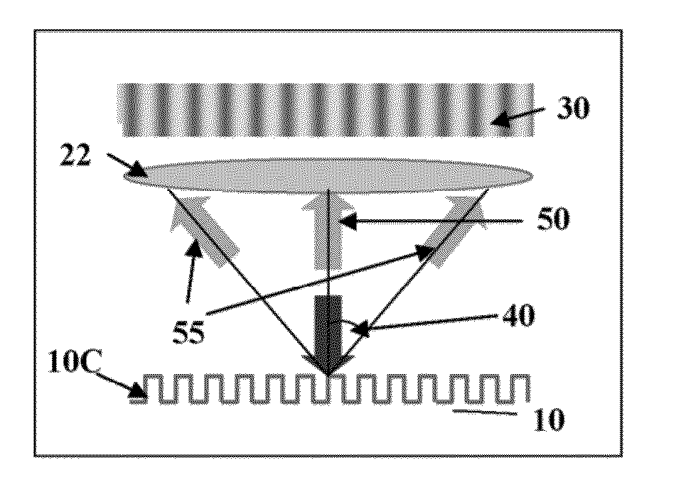
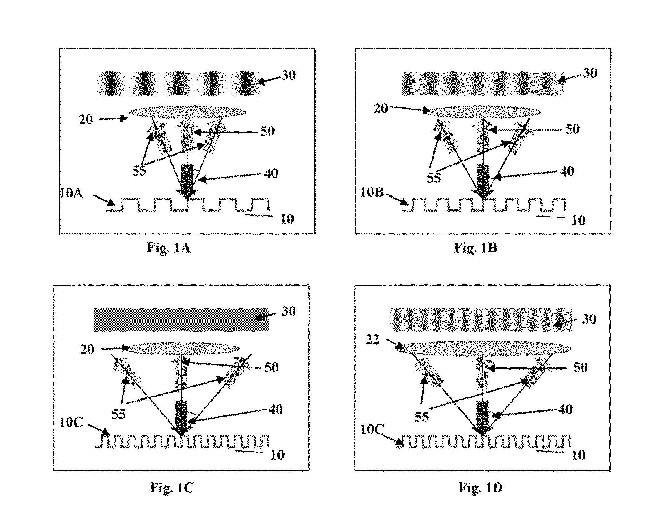
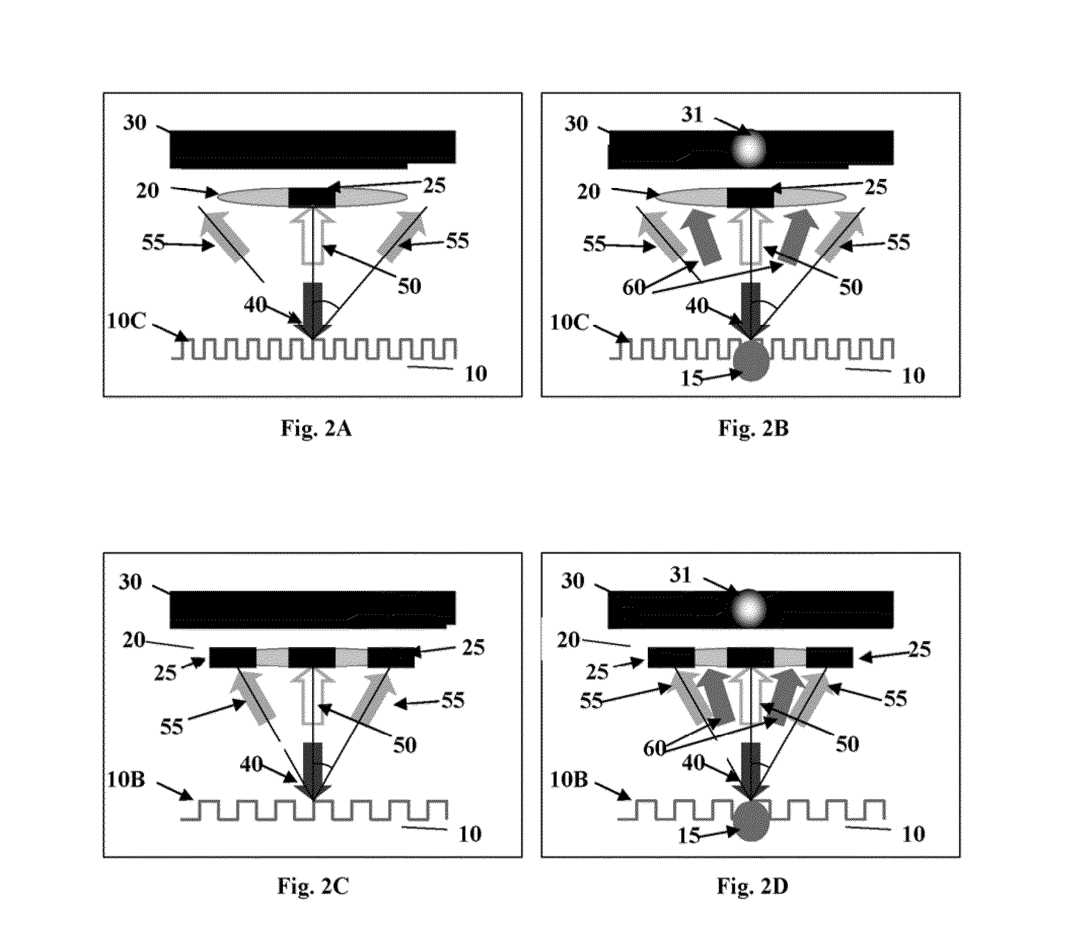
[0047]The general principles of bright field and dark filed inspections of patterned samples are illustrated in FIGS. 1A to 1D and FIGS. 2A to 2D. To facilitate understanding, the same reference numbers are used for identifying components that are common in all the examples.

[0048]It should be noted that, generally, a pattern on the sample's surface may be in a form of a surface relief as shown in FIGS. 1A to 1D, and / or may be defined by regions of different optical properties with respect to given illumination, i.e., regions of different reflection, absorption or transmission properties.

[0049]In FIG. 1A, a sample 10 having a periodic pattern of a certain spatial frequency on its surface 10A is illuminated by an optical beam 40 of a certain wavelength λ (e.g., including ultraviolet and / or infra red illumination) creating an illumination spot on the surface of the sample 10. Light is reflected back from the pattern 10A in different directions according to several diffraction orders. T...


PUM

PropertyMeasurementUnit
optical inspectionaaaaaaaaaa
dimensionaaaaaaaaaa
pitch size dimensionaaaaaaaaaa

Abstract

An optical inspection system for inspecting a patterned sample located in an inspection plane includes an illumination unit defining an illumination channel of a predetermined numerical aperture and first predetermined angular orientation with respect to the inspection plane, and a light collection unit defining a collection channel of second predetermined angular orientation with respect to the inspection plane. The illumination unit comprises an illumination mask located in a first spectral plane with respect to the inspection plane and defining an illumination pupil comprising a first pattern formed by at least one elongated light transmitting region having a physical dimension along one axis larger than along a perpendicular axis. The light collection unit comprises a collection mask located in a second spectral plane with respect to the inspection plane being conjugate to the first spectral plane, the collection mask comprising a second predetermined pattern of spaced-apart light blocking regions.

Description

FIELD OF THE INVENTION[0001]This invention is in the field of optical inspection and relates to a system and method for inspecting patterned samples.BACKGROUND[0002]A decrease in size of the features of a pattern in a semiconductor wafer challenges resolution limits of optical inspection systems. A typical size for features of a pattern corresponding to electronic units is defined by design rules (DRs) of semiconductor wafers.[0003]The shrinking design rules of semiconductor wafers lead to new challenges in optical inspection of the wafer. Pattern inspection techniques typically utilize a so-called bright field (BF) inspection mode.[0004]Traditional BF inspection systems, which are based on resolved imaging of the pattern on a wafer, are limited in their spatial resolution due to diffraction limits of the optics in the imaging system. Using shorter wavelengths, such as the deep ultraviolet (DUV) spectral range, and increasing the numerical aperture (NA) of the imaging system may gen...

Claims


Application Information

Patent Timeline
Patent Type & Authority Applications(United States)
IPC IPC(8): G01N21/956
CPCG01N21/956G01N2021/8822G01N21/4788H01L22/00
Inventor BERLATZKY, YOAVKOFLER, IDOMESHULACH, DORONBARKAN, KOBI
Owner APPL MATERIALS ISRAEL LTD
Why Eureka
Try Eureka