
Method of manufacturing noise removing filter

Inactive Publication Date: 2013-06-20
SAMSUNG ELECTRO MECHANICS CO LTD
View PDF10 Cites 2 Cited by
  • Summary
  • Abstract
  • Description
  • Claims
  • Application Information

AI Technical Summary

Benefits of technology

The present invention provides a method for manufacturing a noise removing filter with high magnetic permeability, excellent adhesive properties, and insulating properties and breakdown voltage properties, thereby increasing impedance characteristics and improving the performance and reliability of the noise removing filter. Additionally, the method simplifies the structure and process of the filter, reducing manufacturing costs and increasing productivity. The method also prevents damage to input / output stud terminals and ensures accuracy in the polishing process.

Problems solved by technology

When data is transmitted between a main device and a peripheral device in a high frequency of GMz band in order to transmit and receive a large amount of data, it is seriously difficult to smoothly process data due to signal delay and other noises.
However, a typical anti-EMI component is a wound or stack type component, has a large chip size, and has low electrical properties, and thus, is used only in a predetermined portion or a limited portion such as a large area circuit board.
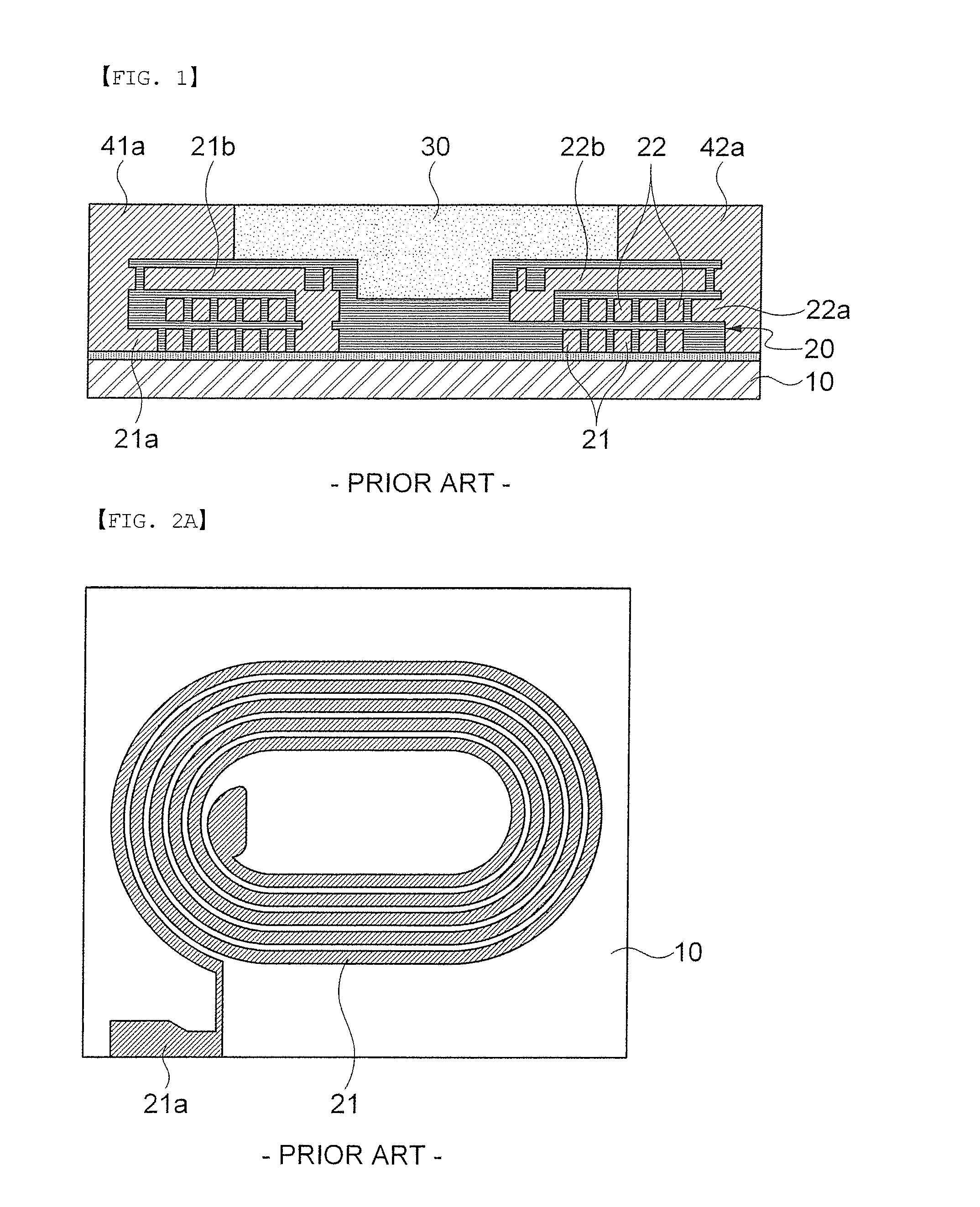
In this case, the magnetic permeability of the common mode filter seriously deteriorates due to the resin included in the upper magnetic body 30, thereby reducing the performance and characteristics of the common mode filter.
However, processability can be reduced at a high temperature, facilities for increasing a temperature can be required, and the reliability of the common mode filter can be reduced.

Method used


Image

  • Method of manufacturing noise removing filter
  • Method of manufacturing noise removing filter
  • Method of manufacturing noise removing filter

Examples


Embodiment Construction

[0044]Hereinafter, the present invention will be described more fully with reference to the accompanying drawings, in which exemplary embodiments of the invention are shown. The invention may, however, be embodied in many different forms and should not be construed as being limited to the embodiments set forth herein; rather, these embodiments are provided so that this disclosure will be thorough and complete, and will fully convey the concept of the invention to those skilled in the art. Throughout this specification, like reference numerals in the drawings denote like elements.

[0045]Unless defined otherwise, technical and scientific terms used herein have the same meaning as is commonly understood by one of skill in the art to which this invention belongs. An expression used in the singular encompasses the expression of the plural, unless it has a clearly different meaning in the context. Also, it is to be understood that the terms such as “comprise” and / or “comprising” are intend...


PUM

PropertyMeasurementUnit
Circumferenceaaaaaaaaaa

Abstract

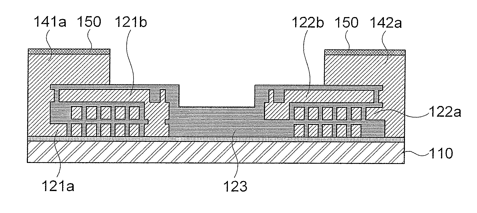
Disclosed herein is a method of manufacturing a noise removing filter, including preparing at least one conductive pattern, an insulating layer for covering the at least one conductive pattern, and a lower magnetic body including input / output stud terminals for electrically inputting and outputting electricity to and from the at least one conductive pattern; disposing a recognizable portion on upper surfaces of the input / output stud terminals; disposing an upper magnetic body on the recognizable portion and the insulating layer; polishing the upper magnetic body; and removing the recognizable portion such that a level of an upper surface of the upper magnetic body is higher than levels of the upper surfaces of the input / output stud terminals.

Description

CROSS REFERENCE(S) TO RELATED APPLICATIONS[0001]This application claims the benefit under 35 U.S.C. Section 119 of Korean Patent Application Serial No. 10-2011-0137426 entitled “Method of Manufacturing Noise Removing Filter” filed on Dec. 19, 2011, which is hereby incorporated by reference in its entirety into this application.BACKGROUND OF THE INVENTION[0002]1. Technical Field[0003]The present invention relates to a noise removing filter, and more particularly, to a method of manufacturing a noise removing filter, by which the noise removing filter may obtain high magnetic permeability so as to improve impedance characteristics by using a simple structure and process, thereby increasing the performance of the noise removing filter.[0004]2. Description of the Related Art[0005]Electronic devices such as digital televisions (TVs), smart phones, or notebook computers have been widely used in terms of data transmission / receiving functions in a high-frequency band. Also, in the future, i...

Claims


Application Information

Patent Timeline
IPC IPC(8): H03H3/00
CPCH03H3/00Y10T29/49169H03H2001/0092G11B5/3163Y10T29/49048Y10T29/49046Y10T29/49044Y10T29/4902Y10T29/49005Y10T29/49147Y10T29/49002Y10T29/49117Y10T29/49069Y10T29/49075H03H1/0007H01F27/00H01F41/00H03H7/01
Inventor LEE, SANG MOONWI, SUNG KWONKWAK, JEONG BOKSIM, WON CHULYOO, YOUNG SEUCKKIM, YONG SUK
Owner SAMSUNG ELECTRO MECHANICS CO LTD
Learn More