Photo detectors

a technology of photo detectors and detectors, applied in the field of photo detectors, can solve the problems of low photocurrent, reduced intensity of incident light irradiated on a single pixel, and inability to improve the integration density of image sensors, so as to achieve enhanced light absorption efficiency and enhanced photoelectric conversion efficiency

Inactive Publication Date: 2013-06-20
ELECTRONICS & TELECOMM RES INST
View PDF9 Cites 6 Cited by
  • Summary
  • Abstract
  • Description
  • Claims
  • Application Information

AI Technical Summary

Benefits of technology

[0008]Exemplary embodiments are directed to photo detectors having an enhanced photoelectric conversion efficiency and / or an enhanced light absorption efficiency.

Problems solved by technology

However, optical systems including optical lenses may be required to realize the images of objects using the CMOS image sensors.
That is, there may be some limitations in improving the integration density of the image sensors.
Further, if the unit pixels are too shrunken down, the intensity of the incident light irradiated on a single pixel is reduced to generate a low photocurrent which is difficult to realize the image.

Method used


Image

  • Photo detectors
  • Photo detectors
  • Photo detectors

Examples


Embodiment Construction

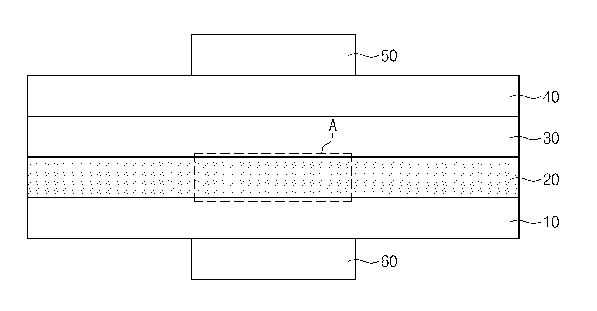
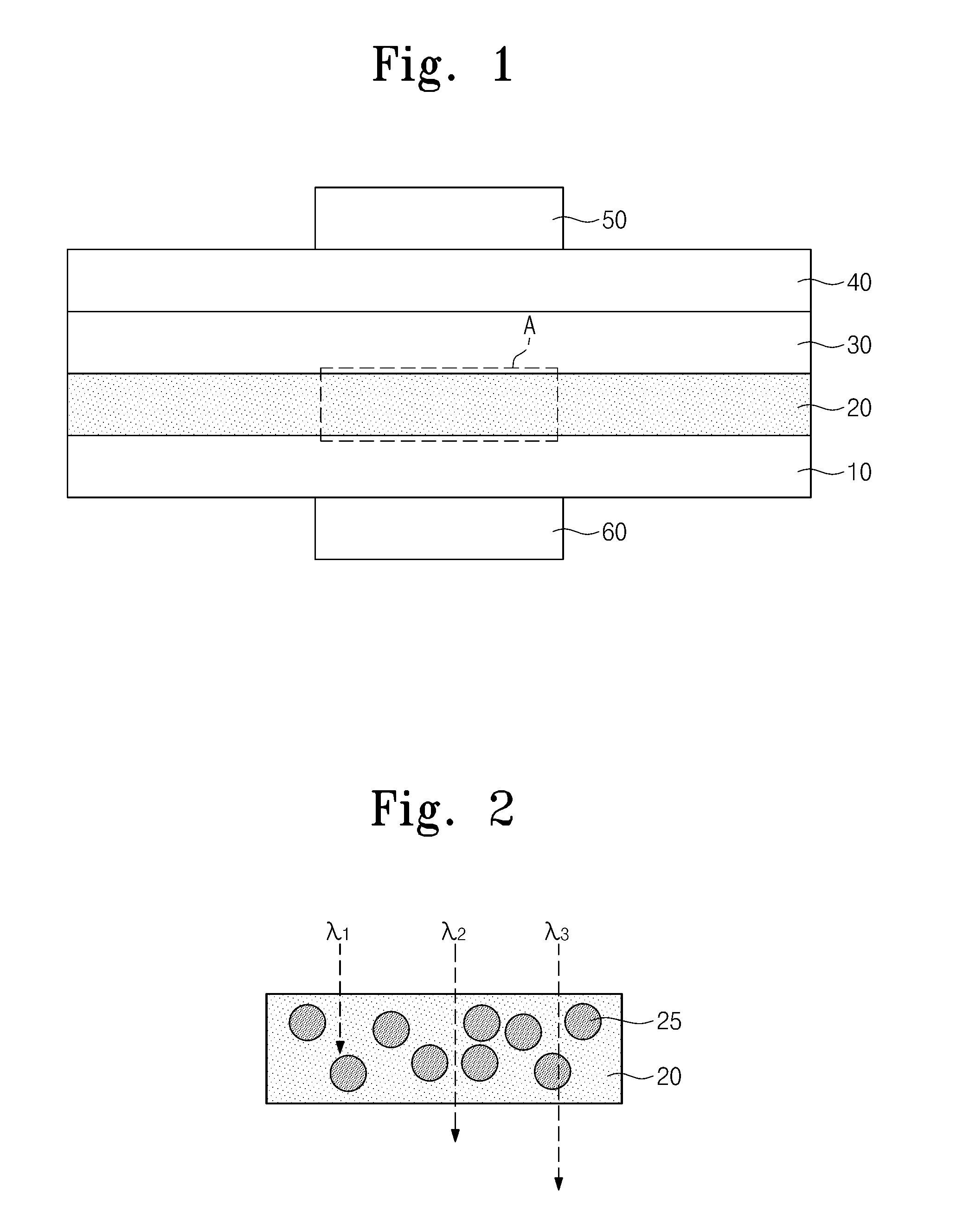
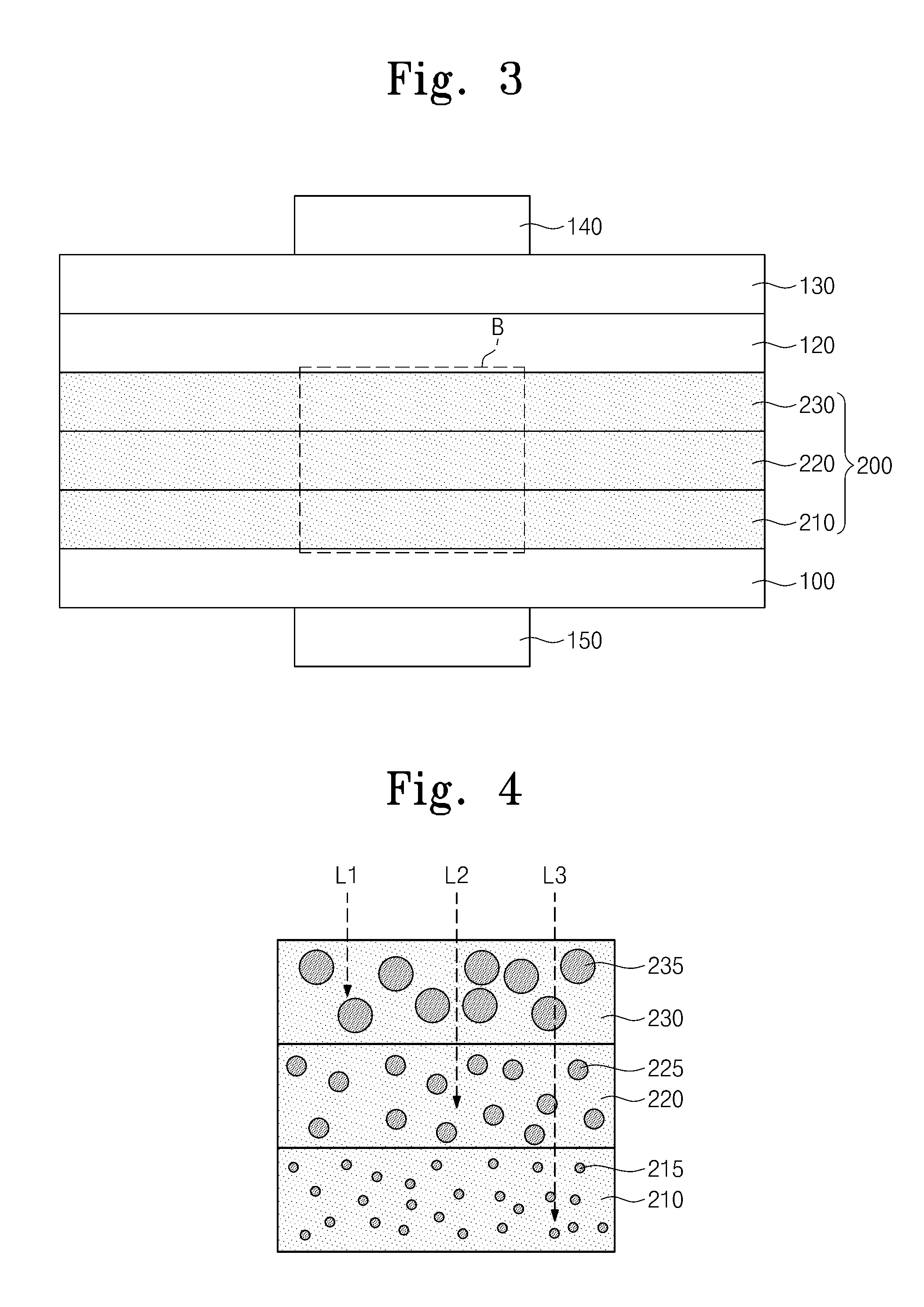
[0028]The inventive concept will now be described more fully hereinafter with reference to the accompanying drawings, in which exemplary embodiments of the inventive concept are shown. The advantages and features of the inventive concept will be apparent from the following exemplary embodiments that will be described in more detail with reference to the accompanying drawings. It should be noted, however, that the inventive concept is not limited to the following exemplary embodiments, and may be implemented in different forms. Rather, these embodiments are provided so that this disclosure will be thorough and complete, and will fully convey the scope of the inventive concept to those skilled in the art.

[0029]It will be understood that when an element such as a layer, region or substrate is referred to as being “on” another element, it can be directly on the other element or intervening elements may be present. In the drawings, the thicknesses of layers and regions are exaggerated fo...


PUM


Abstract

Photo detectors are provided. The photo detector includes a photoelectric conversion layer between a lower carrier transportation layer and an upper carrier transportation layer, and a common electrode on the upper carrier transportation layer opposite to the photoelectric conversion layer. The photoelectric conversion layer includes a plurality of light absorption layers and each of the light absorption layers contains silicon nanocrystals. The silicon nanocrystals in respective ones of the light absorption layers have different sizes from each other.

Description

CROSS-REFERENCE TO RELATED APPLICATIONS[0001]This U.S. non-provisional patent application claims priority under 35 U.S.C. §119 to Korean Patent Application No. 10-2011-0138138, filed on Dec. 20, 2011, the disclosure of which is hereby incorporated by reference in its entirety.BACKGROUND[0002]1. Technical Field[0003]The present disclosure herein relates to photo detectors and, more particularly, to photo detectors having an enhanced photoelectric conversion efficiency.[0004]2. Description of Related Art[0005]Photo detectors, for example, image sensors are semiconductor devices that convert optical signals into electrical signals. The image sensors may include complementary metal-oxide-semiconductor (CMOS) image sensors, and the CMOS image sensors may have some advantages of low fabrication costs, low power consumption, high integration density and high operation speed. Thus, the CMOS image sensors have been continuously developed.[0006]The CMOS image sensors may receive and detect in...

Claims


Application Information

Patent Timeline
Patent Type & Authority Applications(United States)
IPC IPC(8): H01L31/0224B82Y99/00
CPCH01L31/02325B82Y20/00H01L27/14643H01L31/102H01L31/10H01L27/146
Inventor HUH, CHULKIM, SANG HYEOBPARK, BYOUNG-JUNJANG, EUN HYE
Owner ELECTRONICS & TELECOMM RES INST
Why Eureka
Try Eureka