Semiconductor light-emitting element

a technology of light-emitting elements and semiconductors, applied in the field of semiconductor light-emitting elements, can solve the problems of increasing the voltage of the element, increasing the difficulty of the patterning process, and breaking the wiring electrode itself, and achieves the effect of increasing the voltage of the element, and increasing the difficulty of the patterning process

Active Publication Date: 2013-06-27
STANLEY ELECTRIC CO LTD
View PDF2 Cites 51 Cited by
  • Summary
  • Abstract
  • Description
  • Claims
  • Application Information

AI Technical Summary

Benefits of technology

[0007]However, in a conventional light-emitting device such as that described above, if the wiring electrode is gradually made thinner as described in Patent Reference 1, the wiring resistance increases, causing a rise in element-driving voltage. Also, injection of a large current results in heat being generated in the portion at which the wiring electrode is thinner, causing a break in the wiring electrode itself. In addition, making the w

Problems solved by technology

However, in a conventional light-emitting device such as that described above, if the wiring electrode is gradually made thinner as described in Patent Reference 1, the wiring resistance increases, causing a rise in element-driving voltage.
Also, injection of a large current results in heat being generated in the portion at which the wiring electrode is thinner, causing a break in the wiring electrode itself.
In addition, making the wiri

Method used


Image

  • Semiconductor light-emitting element
  • Semiconductor light-emitting element
  • Semiconductor light-emitting element

Examples


first embodiment

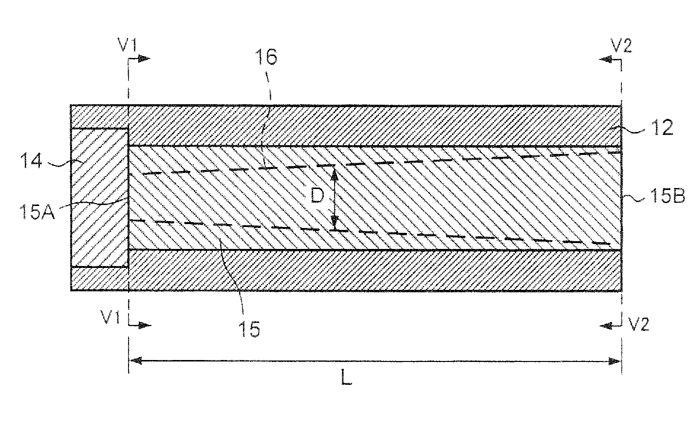
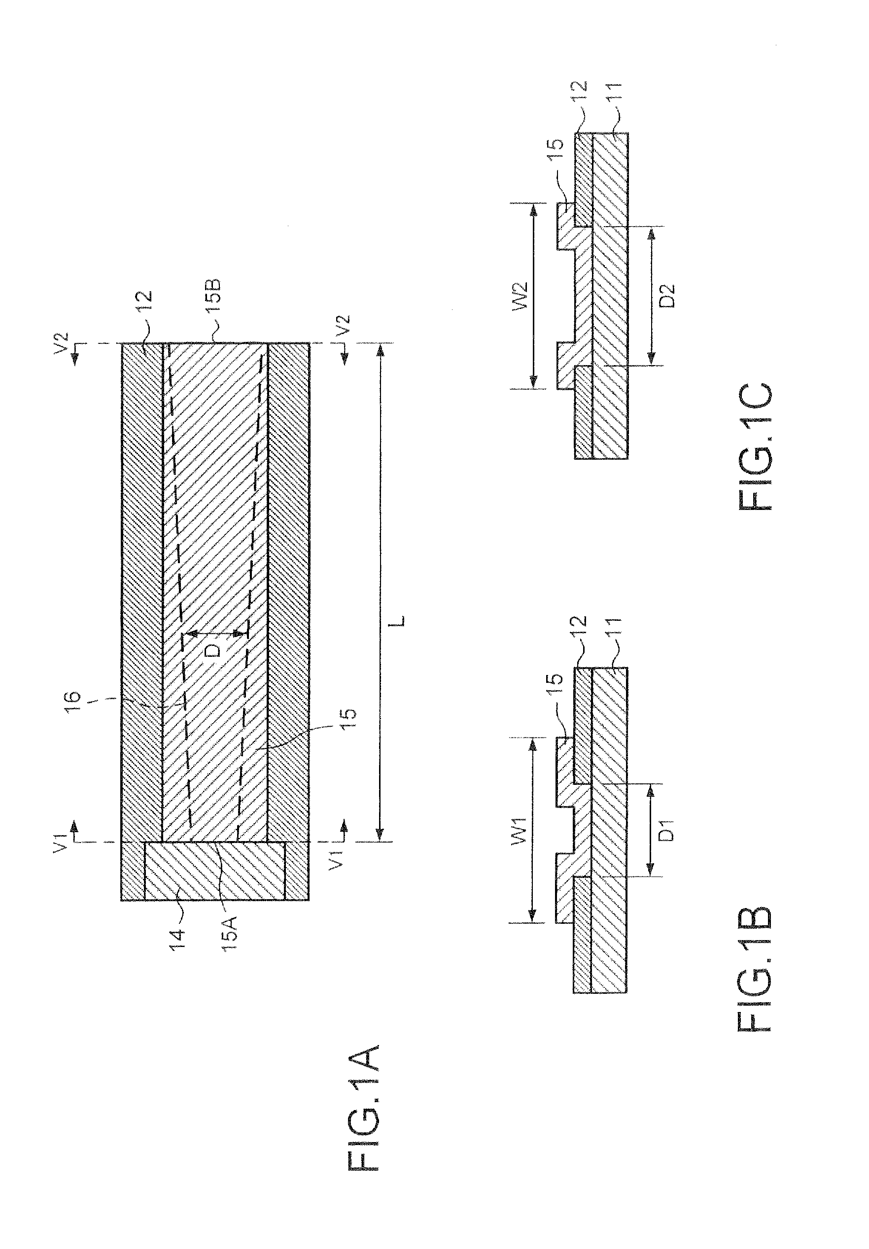
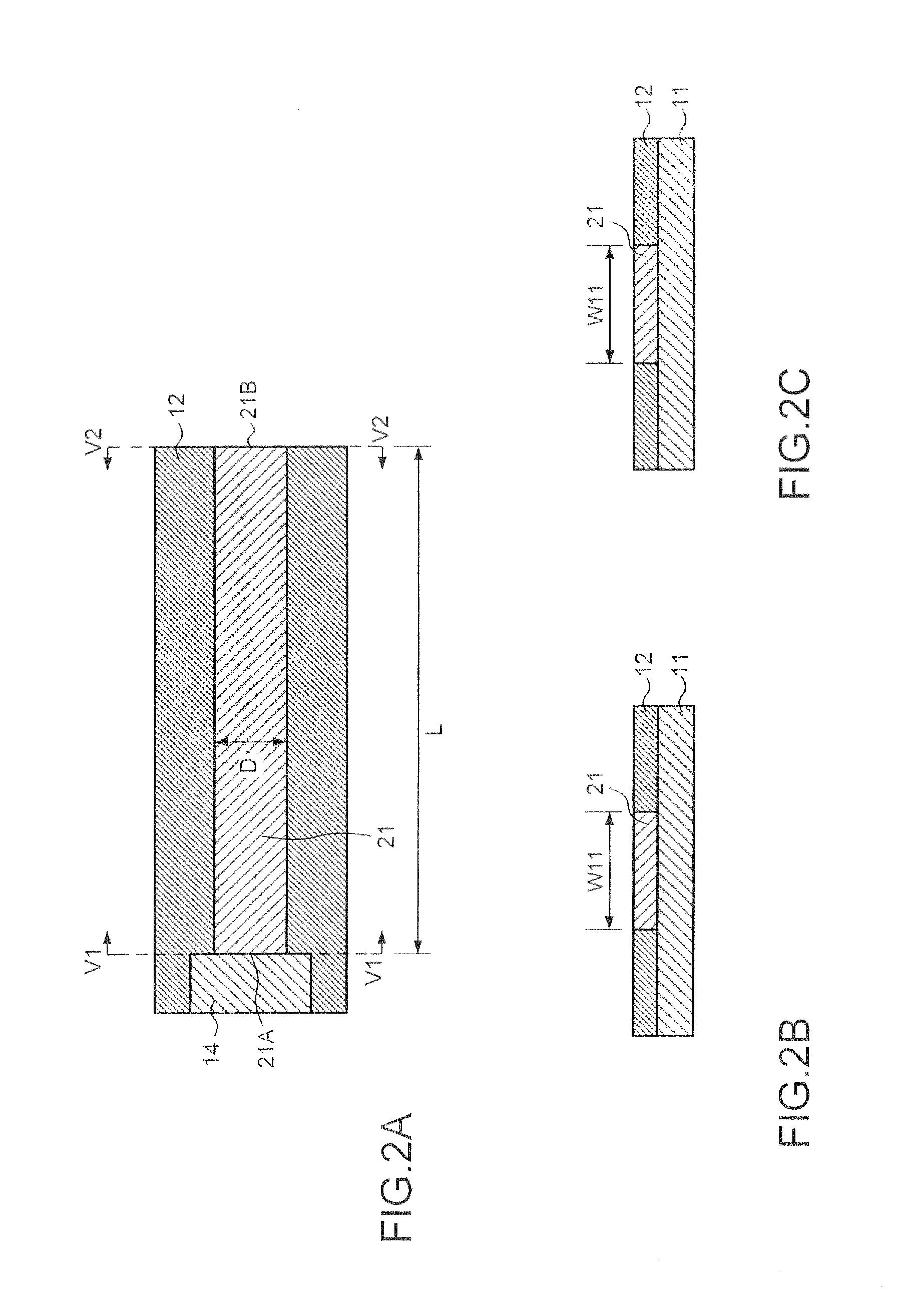
[0027]FIG. 1A is a too view schematically illustrating the basic electrode structure (hereafter also referred to as “electrode structure E1”) according to a first embodiment of the invention; and FIGS. 1B and 1C are cross-section views schematically illustrating the cross-section along line V1-V1 and V2-V2 of FIG. 1A respectively. In detail, an insulation layer 12 is formed on a semiconductor layer 11. A pad electrode 14, which is a connection electrode connected by a bonding wire or a similar element to an external circuit and which receives supply of a current, is formed on the insulation layer 12. A wiring electrode 15, electrically connected to the pad electrode 14, is also formed. The wiring electrode 15 stretches or extends on the insulation layer 12 along the surface of the semiconductor layer 11 from the connection portion at which a connection is established with the pad electrode 14, and has a width W1 at the connection portion and a width W2 at a terminal end portion (dis...

second embodiment

[0042]FIGS. 9A and B are a top view of an electrode structure (hereafter also referred to as “E2”) according to a second embodiment of the invention and a partial cross-section views of an LED 50 having the electrode structure E2. FIG. 9B schematically illustrates the cross-section of a portion (i.e., region P1 indicated by a dashed line) of FIG. 9A. As shown in FIG. 9B, the LED 50 is formed by forming a semiconductor layered body comprising AlGaInP-based semiconductor layers on a C-plane sapphire or another growth substrate using e.g., metal-organic chemical vapour deposition (MOCVD); then bonding the semiconductor layered body with an Si or another support substrate; interposed by a bonding layer; and removing the growth substrate using laser-lift-off (LLO) or another method. In more detail, the LED 50 comprises a support substrate 51, a bonding layer 52, a light-reflecting film 53, a transparent electrode layer (p-electrode) 54, a p-type semiconductor layer 55, a light-emitting l...

third embodiment

[0054]In the abovementioned first and second embodiments, descriptions were given for instances in which the width of the contact region in which the wiring electrode is in contact with the semiconductor layer increases from the connecting portion with the connection electrode (e.g., pad electrode) along the direction in which the wiring electrode is stretched; however, this is not provided by way of limitation. It is only necessary that a configuration is present in which the contact area of the wiring electrode increases in an equivalent manner along the direction in which the wiring electrode is stretched without the width of the wiring electrode being reduced.

[0055]FIG. 13A is a top view schematically illustrating an electrode structure, according to a third embodiment of the present invention (hereafter also referred to as “electrode structure; E3”), representing an example of a wiring electrode configured so that the contact area increases in an equivalent manner. FIGS. 13B an...


PUM


Abstract

There is provided a semiconductor light-emitting element which has an electrode structural body including a connection electrode and a wiring electrode connected to the connection electrode, the wiring electrode stretching along a surface of a semiconductor layered body while being in partial contact with the surface of the semiconductor layered body exposed from an opening formed on the insulation layer. The area of a contact region between the wiring electrode and the semiconductor layered body increases, from a connection end which is connected to the connection electrode, along a direction in which the wiring electrode stretches.

Description

BACKGROUND OF THE INVENTION[0001]1. Field of the Invention[0002]The present invention relates to a light-emitting element, and in particular to a semiconductor light-emitting element such as a light-emitting diode (LED).[0003]2. Description of the Related Art[0004]Conventionally, in a semiconductor light-emitting element such as a light-emitting diode (LED), a pad electrode or another connection electrode is provided on the semiconductor layer (or a contact layer) on the surface of the element. Supply current from the exterior is injected into the semiconductor light-emitting element through the connection electrode and the light-emitting element is caused to emit light. There is used a configuration in which a wiring electrode connected to the connection electrode is provided on the contact layer, and a current is injected into the semiconductor light-emitting element.[0005]In an LED in which the surface of the semiconductor light-emitting element is the light-extraction surface, i...

Claims


Application Information

Patent Timeline
IPC IPC(8): H01L33/36
CPCH01L33/36H01L33/44H01L33/38
Inventor LIANG, JI-HAOKAWAI, RYOSUKE
Owner STANLEY ELECTRIC CO LTD
Why Eureka
Try Eureka