Method of manufacturing light emitting device, and light emitting device

Active Publication Date: 2013-06-27
NICHIA CORP
View PDF9 Cites 5 Cited by
  • Summary
  • Abstract
  • Description
  • Claims
  • Application Information

AI Technical Summary

Benefits of technology

[0011]A method of manufacturing a light emitting device according to the aspects of the present invention enables high accuracy mounting of a plurality of light e

Problems solved by technology

However, although a technique of mounting a large planar dimension light emitting element on a package or the like is relatively easy to perform, production of such a light emitting element having a large planar dimension from a wafer with good yield is difficult.
However, an arrangement of the plurality of light emitting elemen

Method used


Image

  • Method of manufacturing light emitting device, and light emitting device
  • Method of manufacturing light emitting device, and light emitting device
  • Method of manufacturing light emitting device, and light emitting device

Examples


Example

EMBODIMENT 1

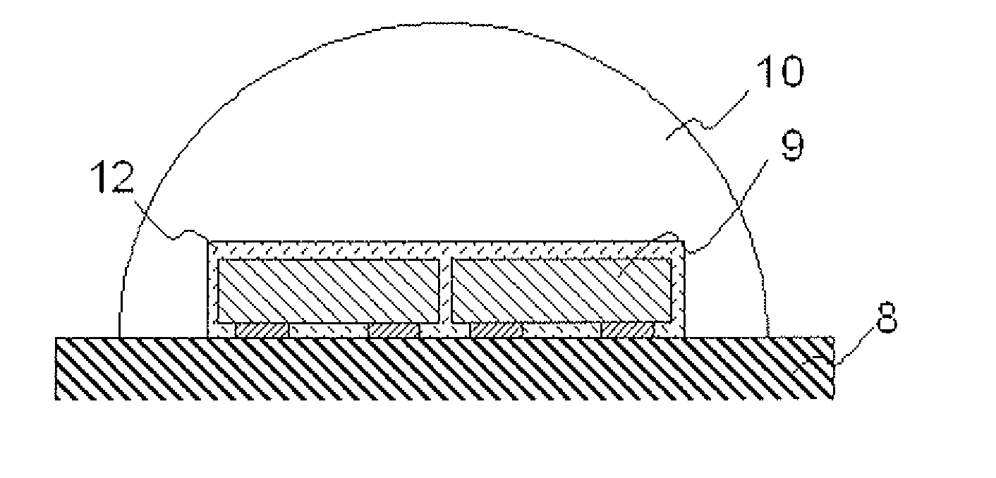
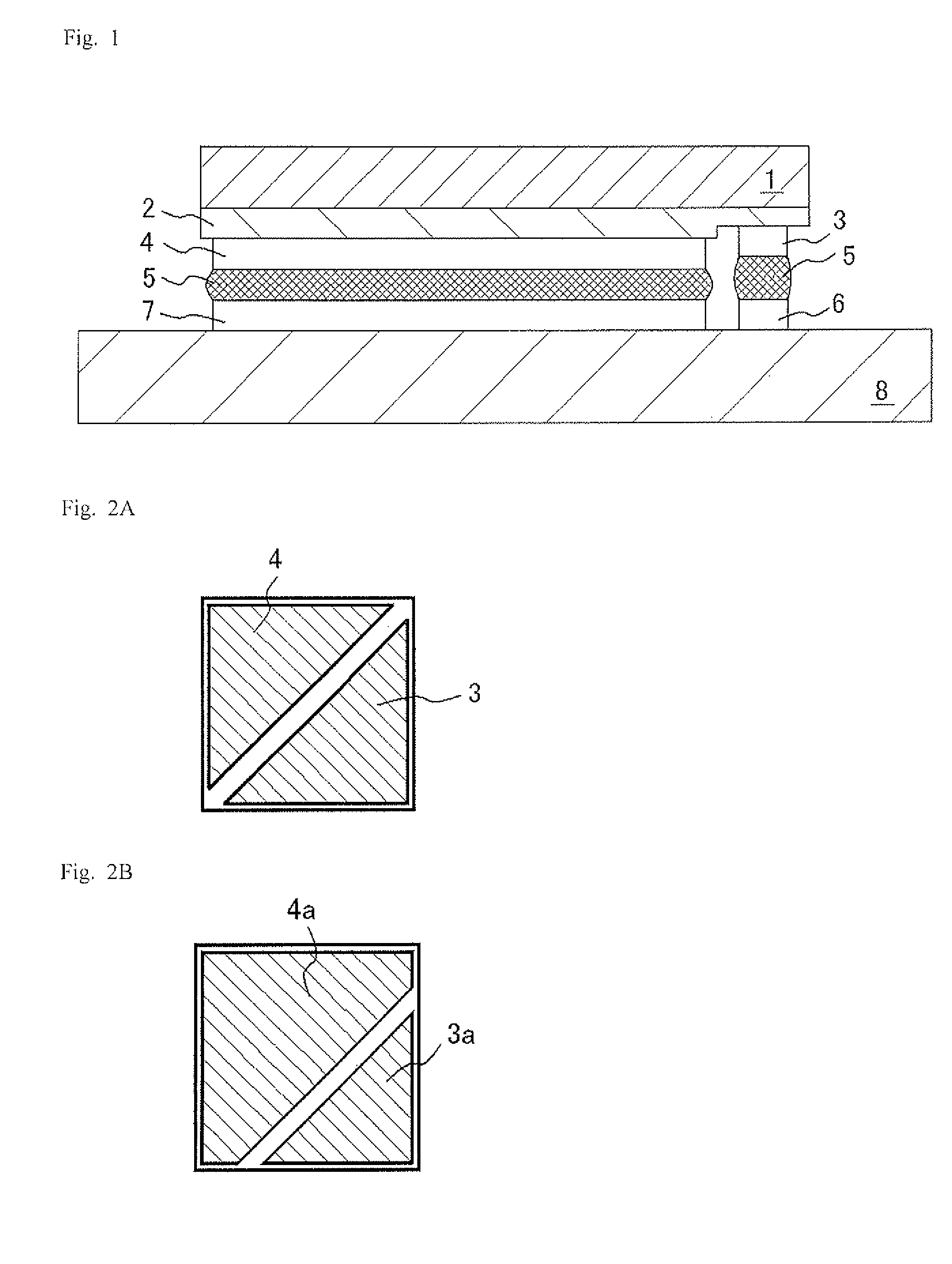
[0055]In order to mount a light emitting element on a support substrate 8 having a group of electrically conductive members disposed on its surface as shown in FIG. 1, firstly, a light emitting element and a support substrate 8 are prepared. The light emitting element has a size of, for example in a plan view, about 1.0 mm×1.0 mm. The first electrode 3 and the second electrode 4 of the light emitting element have, as shown in FIG. 2A. approximately the same planar dimension. For the support substrate 8, an alumina ceramic substrate is used. The support substrate 8 is cut in a final process to obtain individual light emitting devices with a size of approximately 3.0 mm×3.0 mm. Hereinafter, a single light emitting device will be described, but in a practical sense, a plurality of light emitting devices are processed simultaneously before dividing into individual devices. On the surface of the support substrate 8, a group of electrically conductive members made up of six pi...

Example

EMBODIMENT 2

[0059]The light emitting device was fabricated in the same manner as in Embodiment I except that the pattern of the group of electrically conductive members had a shape as shown in FIG. 4. As a result, in the same manner as in Embodiment 1, a distance of less than 20 μm between the light emitting elements was achieved.

Example

EMBODIMENT 3

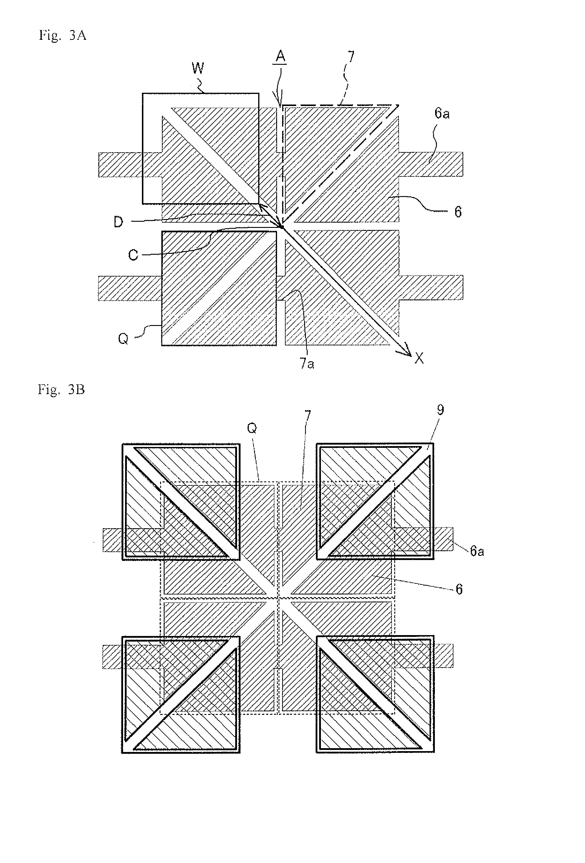
[0060]The light emitting device is fabricated in the same manner as in Embodiment 1 except for using the light emitting elements having the shapes of the first element electrode 3a and the second element electrode 4a as shown in FIG. 2B and employing a pattern of the group of electrically conductive members as shown in FIG. 5A, and placing the light emitting elements 9 with the light emitting elements 9 being shifted with respect to the intended positions Q as shown in FIG. 5B. As a result, in the same manner as in Embodiment 1, a distance of less than 20 μm between the light emitting elements can be achieved. Further, occurrence of short circuit between the electrodes can be prevented.


PUM

PropertyMeasurementUnit
Fractionaaaaaaaaaa
Fractionaaaaaaaaaa
Thicknessaaaaaaaaaa

Abstract

A method of manufacturing a light emitting device includes: disposing a group of electrically conductive members on a support substrate, the group of the electrically conductive members forming a plurality of mounting portions arranged in two or more columns and two or more rows with the mounting portions respectively corresponding to a plurality of light emitting elements; placing the light emitting elements on the group of the electrically conductive members with a bonding member being disposed between the light emitting elements and the electrically conductive members, each of the light emitting elements being shifted from a corresponding one of the mounting portions; and melting the bonding member to mount the light emitting elements respectively on the mounting portions by self-alignment effect generated by the melting of the bonding member.

Description

BACKGROUND OF THE INVENTION[0001]1. Field of the Invention[0002]The present invention relates to a method of manufacturing a light emitting device and a light emitting device.[0003]2. Background Information[0004]There has been used a surface mount type light emitting device, in which a light emitting element such as a light emitting diode (LED) or a laser diode (LD) is mounted on a substrate. Such light emitting devices are used for lighting apparatus, backlight of display screen, light source for vehicle, light source for display, auxiliary light source for moving images, and other general consumer light sources. As compared with conventional light sources, such light emitting devices have a longer life and are capable of emitting light under an energy-serving environment, which are attracting high expectation as a next generation light source for lighting applications.[0005]In recent years, even higher levels of output powder is in demand, and in order to comply, increase in size ...

Claims


Application Information

Patent Timeline
IPC IPC(8): F21V21/00F21V7/00F21V9/16
CPCF21V21/00F21V9/16Y10T29/49117H01L33/0079H01L2933/0066F21V7/00F21V9/30F21V13/14H01L33/0093H01L2224/14H01L2224/16225H01L25/0753H01L33/62
Inventor SUZUKI, RYO
Owner NICHIA CORP
Why Eureka
Try Eureka