Two-wire load control device for low-power loads

a load control device and load technology, applied in the field of electronic switches, can solve the problems of increasing the cost of prior art fet-based reverse phase-control dimmer switches, load to illuminate, and high-efficiency light sources typically consume less power and provide longer operational li

Active Publication Date: 2013-07-04
LUTRON TECH CO LLC
View PDF4 Cites 82 Cited by
  • Summary
  • Abstract
  • Description
  • Claims
  • Application Information

AI Technical Summary

Problems solved by technology

However, prior art reverse phase-control dimmer switches have either required neutral connections and / or advanced control circuits (such as microprocessors) for controlling the operation of the FETs.
These advanced control circuits and power supplies add to the cost of prior art FET-based reverse phase-control dimmer switches (as compared to analog forward phase-control dimmer switches).
If the power rating of the lighting load is too low, the charging current conducted by the power supply through the lighting load may be great enough to cause the lighting load to illuminate to a level that is perceptible to the human eye when the lighting load is off.
High-efficiency light sources typically consume less power and provide longer operational lives as compared to incandescent and halogen lamps.
However, the load regulation devices for the high-efficiency light sources may have high input impedances or input impedances that vary in magnitude throughout a half cycle.
Therefore, when a prior-art forward phase-control dimmer switch is coupled between the AC power source and the load regulation device for the high-efficiency light source, the load control device may not be able to conduct enough current to exceed the rated latching and / or holding currents of the thyristor.
In addition, when a prior-art reverse phase-control dimmer switch is coupled between the AC power source and the load regulation device, the magnitude of the charging current of the power supply may be great enough to cause the load regulation device to illuminate the controlled high-efficiency light source to a level that is perceptible by the human eye when the light source should be off.
The impedance characteristics of the load regulation device may negatively affect the magnitude of the phase-control voltage received by the load regulation device, such that the conduction time of the received phase-control voltage is different from the actually conduction time of the bidirectional semiconductor switch of the dimmer switch (e.g., if the load regulation device has a capacitive impedance).
In addition, the charging current of the power supply of the dimmer switch may build up charge at the input of a load regulation device having a capacitive input impedance, thus negatively affecting the low-end intensity that may be achieved.

Method used


Image

  • Two-wire load control device for low-power loads
  • Two-wire load control device for low-power loads
  • Two-wire load control device for low-power loads

Examples


first embodiment

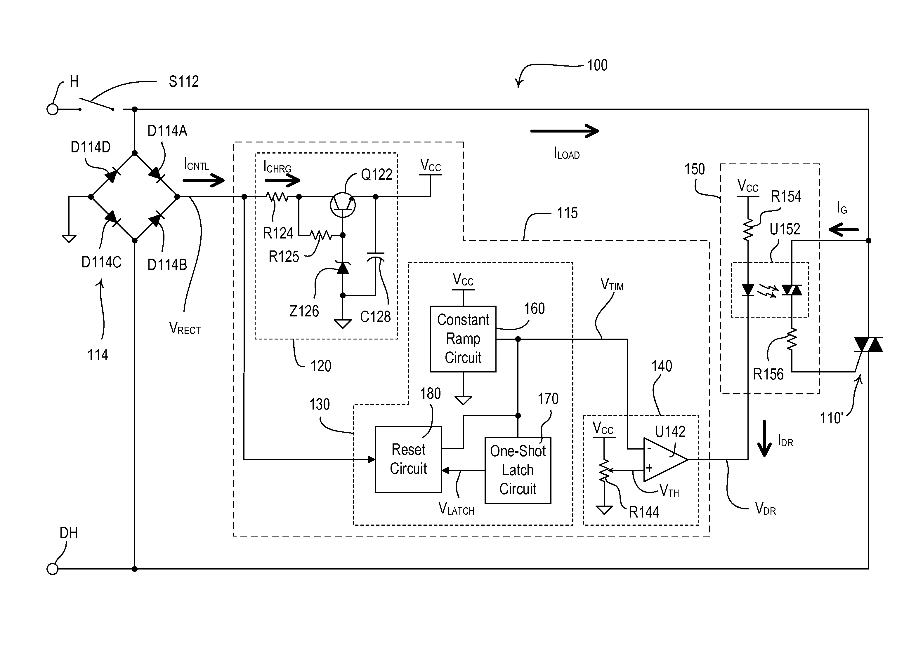
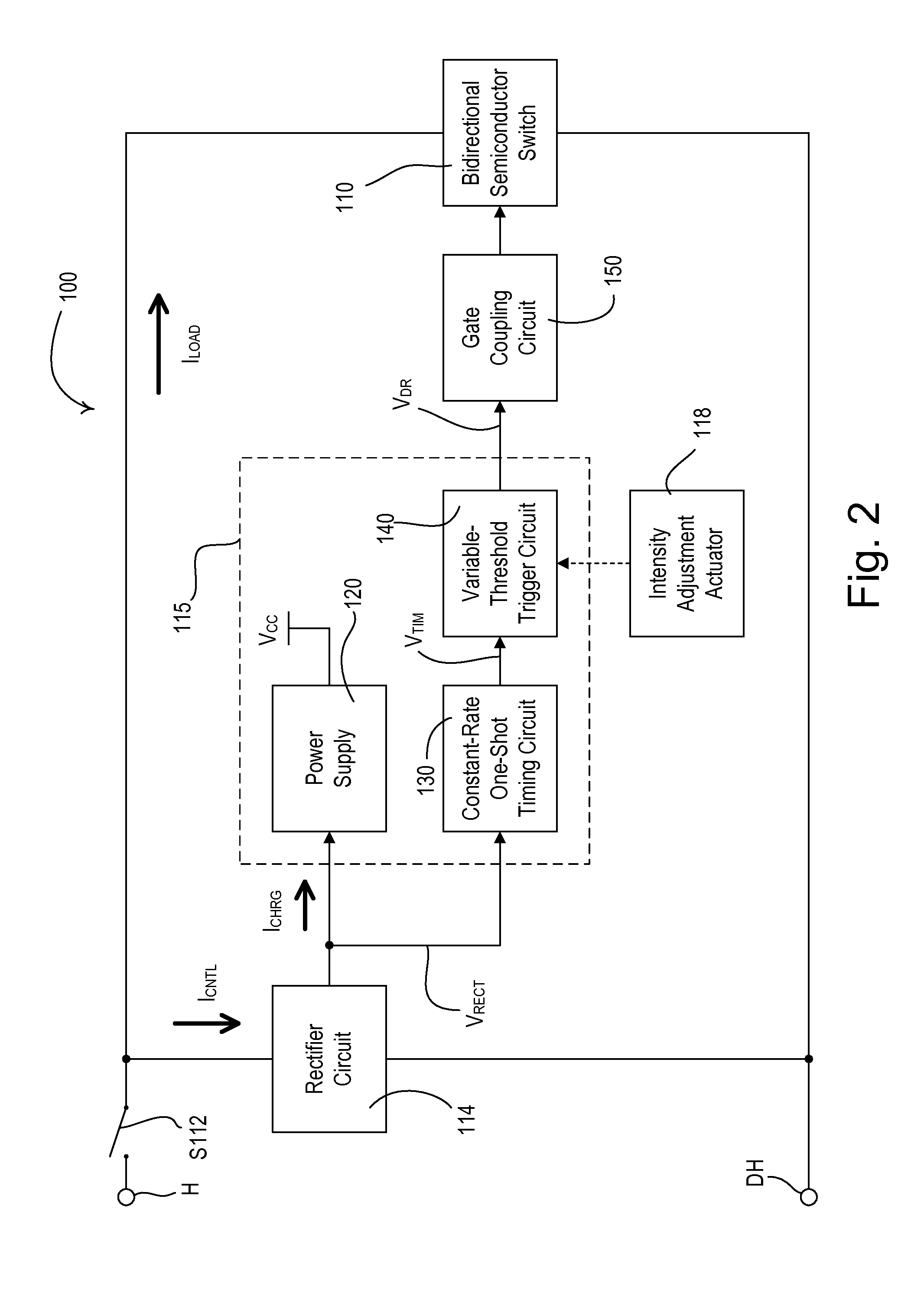
[0059] the dimmer switch 100 comprises an analog control circuit 115 including a power supply 120, a constant-rate one-shot timing circuit 130, and a variable-threshold trigger circuit 140 (i.e., a gate drive circuit). The control circuit 115 receives the rectified voltage VRECT from the rectifier circuit 114 and conducts a control current ICNTL through the load (i.e., the LED driver 102) in order to generate a drive voltage VDR (i.e., a drive signal) for controlling the bidirectional semiconductor switch 110 to thus adjust the intensity of the LED light source 104 in response to the intensity adjustment actuator 118. The power supply 120 of the control circuit 115 conducts a charging current ICHRG through the LED driver 102 in order to generate a supply voltage VCC (e.g., approximately 11.4 volts). The charging current ICHRG of the power supply makes up a portion of the control current ICNTL of the control circuit 115.

[0060]The timing circuit 130 receives the supply voltage VCC and...

third embodiment

[0093]In addition, the dimmer switch 300 of the third embodiment does not require the opto-coupler U152 to render the triac 110′ conductive. As previously mentioned, the opto-coupler U152 is typically expensive and is characterized by the rated turn-on time, which limits how quickly the triac 110′ can be rendered conductive after becoming non-conductive in response to the load current ILOAD changing directions.

[0094]Since the magnitude of the gate current IG conducted by the FETs Q352A, Q352B of the gate coupling circuit 350 is much less than the magnitude of the load current ILOAD conducted by the triac 110′, the FETs Q352A, Q352B of the third embodiment may be sized smaller in power rating (and accordingly, in physical size) than the FETs Q210A, Q210B of the dimmer switch 200 of the second embodiment (which conduct the load current ILOAD). In other words, because the FETs Q352A, Q352B of the third embodiment do not conduct the load current ILOAD, the FETs need not be power devices...

fourth embodiment

[0097]FIG. 10 is a simplified timing diagram showing examples of the phase-control voltage VPC generated by the dimmer switch 400, the timing voltage VTIM, and the gate voltage VG for driving the FETs Q210A, Q210B according to the present invention. The phase-control voltage VPC has a magnitude equal to approximately the magnitude of the AC line voltage VAC of the AC power source 105 at the beginning of each half cycle during a conduction time TCON, and has a magnitude of approximately zero volts during the rest of the half cycle, i.e., during a non-conduction time TNC. To generate the phase-control voltage VPC, the gate drive circuit 440 drives the gate voltage VG high towards the reference voltage VREF at the beginning of each half cycle, such that the FETs Q210A, Q210B are rendered conductive (as shown at time t1 in FIG. 10). At this time, the timing circuit 430 begins generating the timing voltage VTIM, which comprises a ramp voltage that increases in magnitude with respect to t...


PUM


Abstract

A two-wire load control device (such as, a dimmer switch or an electronic switch) for controlling the power delivered from an AC power source to an electrical load includes a controllably conductive device for controlling the power to the load, a microprocessor operable to generate a control signal that is representative of whether the load should be controlled on or off, a capacitor operable to produce a supply voltage for powering the microprocessor, a power supply that charges the capacitor when the controllably conductive device is non-conductive, and a control circuit that receives the control signal from the microprocessor. The control circuit is operatively coupled to the controllably conductive device for maintaining the controllably conductive device non-conductive after the beginning of each half-cycle until the magnitude of the supply voltage exceeds a predetermined threshold.

Description

[0001]This is a continuation-in-part of commonly-assigned U.S. patent application Ser. No. 13 / 458,324, filed Apr. 27, 2012, entitled TWO-WIRE DIMMER SWITCH FOR LOW-POWER LOADS, which is a continuation-in-part of U.S. patent application Ser. No. 13 / 232,344, filed Sep. 14, 2011, entitled TWO-WIRE DIMMER SWITCH FOR LOW-POWER LOADS, which is a continuation-in-part of U.S. patent application Ser. No. 12 / 952,920, filed Nov. 23, 2010, entitled TWO-WIRE DIMMER SWITCH FOR LOW-POWER LOADS, which claims priority from U.S. Provisional Patent Application No. 61 / 264,528, filed Nov. 25, 2009, and U.S. Provisional Patent Application No. 61 / 333,050, filed May 10, 2010, both entitled TWO-WIRE ANALOG DIMMER SWITCH FOR LOW-POWER LOADS, the entire disclosures of which are hereby incorporated by reference.BACKGROUND OF THE INVENTION[0002]1. Field of the Invention[0003]The present invention relates to load control devices for controlling the amount of power delivered to an electrical load, and more partic...

Claims


Application Information

Patent Timeline
Patent Type & Authority Applications(United States)
IPC IPC(8): H02M7/06H05B44/00
CPCH02M7/06H05B33/0815Y02B20/346H05B39/044H05B39/048H05B39/04Y02B20/00Y02B20/30H05B45/38H05B45/375H05B45/10H05B47/16
Inventor NEWMAN, JR., ROBERT C.CARMEN, DANIEL F.
Owner LUTRON TECH CO LLC
Why Eureka
Try Eureka