Component built-in module, electronic device including same, and method for manufacturing component built-in module

a technology of built-in modules and electronic devices, applied in the direction of printed circuit manufacturing, printed circuit aspects, semiconductor/solid-state device details, etc., can solve the problem of becoming difficult to realize further low-profiling, and achieve the effect of preventing separation between the substrate and the resin (sealing resin), high reliability, and high reliability

Active Publication Date: 2013-07-11
LENOVO INNOVATIONS LTD HONG KONG
View PDF1 Cites 23 Cited by
  • Summary
  • Abstract
  • Description
  • Claims
  • Application Information

AI Technical Summary

Benefits of technology

[0020]In the component built-in module, the electronic device including it, and the method for manufacturing a component built-in module of the present invention, the component built-in module is formed such that the resin that seals the top surface (one side) of the substrate is bonded to the reinforcing plate provided on the bottom surface side of the substrate. As a result, separation between the substrate and the resin (sealing resin) can be prevented.
[0021]Moreover, in an exemplary embodiment of the present invention, this type of component built-in module serves as at least a part of the casing of the electronic device. That is to say, the plurality of electronic components of the component built-in module are embedded within the casing of the electronic device. With this configuration, further low-profiling of the electronic device can be realized.
[0022]As a result, it is possible to provide a highly reliable component built-in module and an electronic device including it while low-profiling can be achieved and separation between the substrate and the resin can be prevented.

Problems solved by technology

With a structure such as one seen in a mobile phone in which components including a plurality of component built-in modules, a display, and a battery are accommodated within a preliminarily prepared casing, it is becoming difficult to realize further low-profiling.

Method used


Image

  • Component built-in module, electronic device including same, and method for manufacturing component built-in module
  • Component built-in module, electronic device including same, and method for manufacturing component built-in module
  • Component built-in module, electronic device including same, and method for manufacturing component built-in module

Examples


first exemplary embodiment

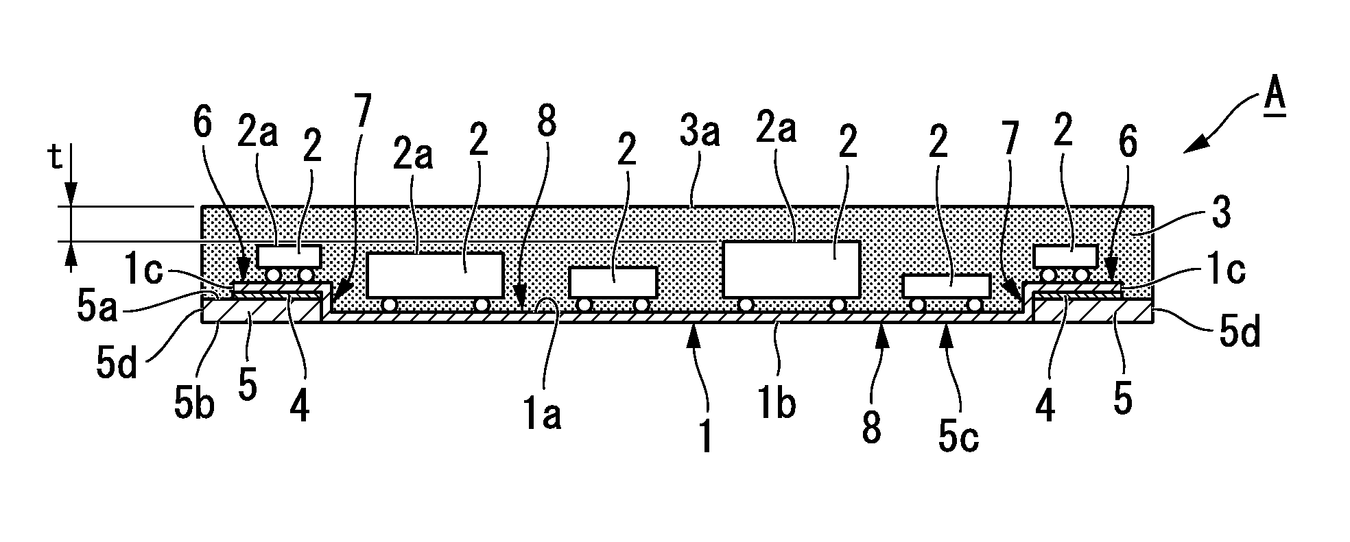
[0038]Hereunder, a component built-in module according to an exemplary embodiment of the present invention, an electronic device including it, and a method for manufacturing a component built-in module are described, with reference to FIG. 1 through FIG. 4E. The present exemplary embodiment relates to a component built-in module to be equipped in an electronic device that requires low-profiling such as a mobile phone, an electronic device, and a method for manufacturing a component built-in module.

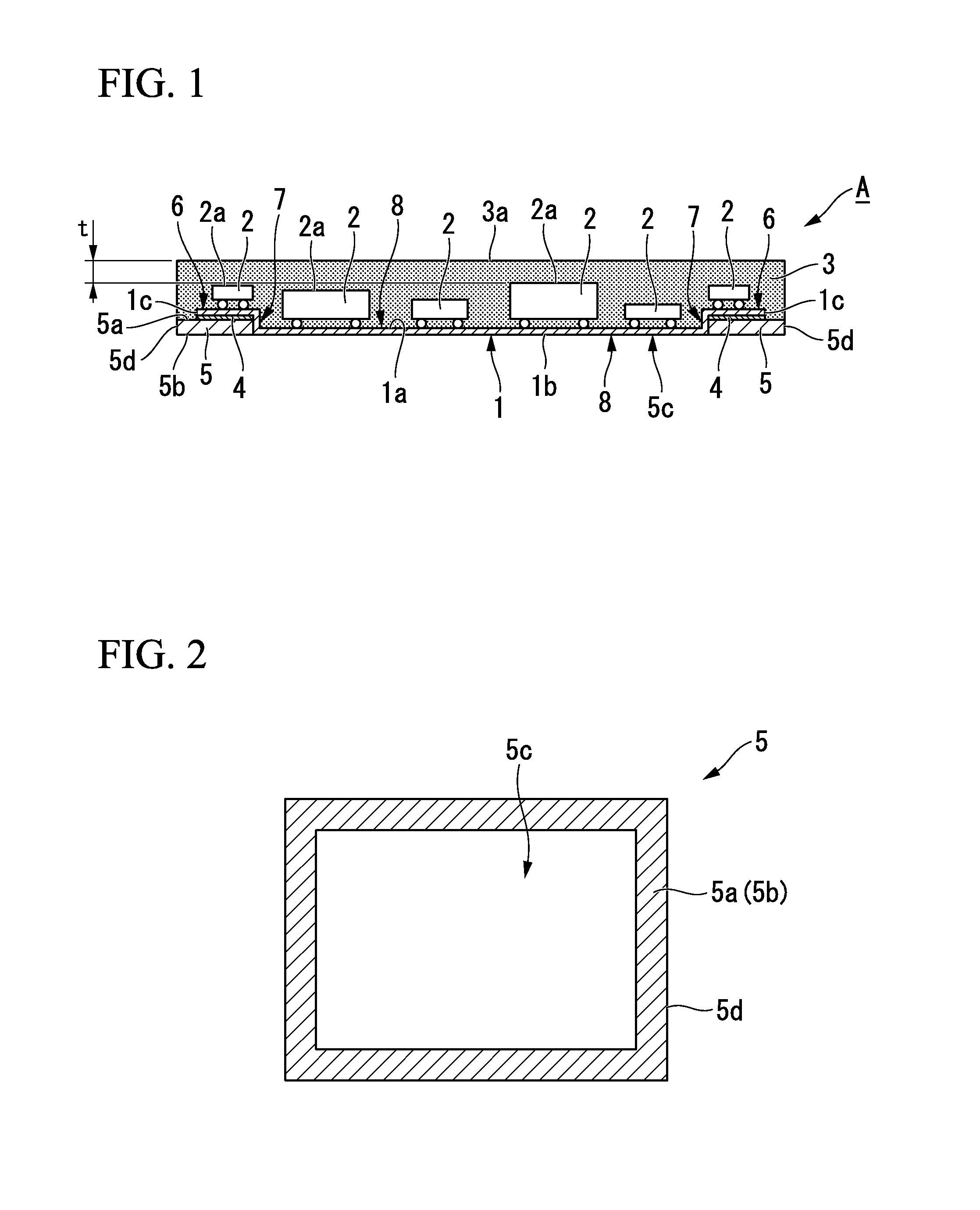
[0039]As shown in FIG. 1, a component built-in module A of the present exemplary embodiment includes: a substrate (wiring substrate) 1, a plurality of electronic components 2, a resin 3, and a reinforcing plate 5. The substrate 1 is for example a flexible substrate. The substrate 1 has a top surface (mounting surface) 1a and a bottom surface 1b on the opposite side to the top surface 1a. The plurality of electronic components 2 are mounted on the top surface 1a of the substrate 1. The resi...


PUM

PropertyMeasurementUnit
thicknessaaaaaaaaaa
distanceaaaaaaaaaa
bonding widthaaaaaaaaaa

Abstract

A component built-in module of the present invention includes: a substrate which includes a top surface and a bottom surface; a plurality of electronic components which are mounted on the top surface of the substrate; a resin which seals the top surface of the substrate; and a reinforcing plate which is bonded to the bottom surface of the substrate. The reinforcing plate and the resin are bonded to each other.

Description

TECHNICAL FIELD[0001]The present invention relates to a component built-in module in which a substrate having a plurality of electronic components mounted thereon is sealed with a resin, an electronic device including it, and a method for manufacturing a component built-in module.BACKGROUND ART[0002]For example, an electronic device such as a mobile phone includes a casing including an upper casing and a lower casing each composed of a synthetic resin, a plurality of component built-in modules that each have a plurality of electronic components mounted thereon and that are accommodated within the casing, a display, and a battery.[0003]Meanwhile, with the recent full scale arrival of an ubiquitous network society there has been an increasing demand for downsizing and low-profiling of electronic devices. With a structure such as one seen in a mobile phone in which components including a plurality of component built-in modules, a display, and a battery are accommodated within a prelimi...

Claims


Application Information

Patent Timeline
Patent Type & Authority Applications(United States)
IPC IPC(8): H05K7/02H05K3/30
CPCH05K3/284H05K2201/2009H05K2201/2018H05K2203/1316H01L21/565Y10T29/4913H01L21/561H01L2224/16225H05K3/305H05K7/02H01L23/3121
Inventor NISHIMURA, NOZOMUMIKAMI, NOBUHIRO
Owner LENOVO INNOVATIONS LTD HONG KONG
Why Eureka
Try Eureka