Film forming method

a film and thin film technology, applied in the field of thin film forming methods, can solve the problems of poor step coverage, poor film forming rate, inconsistent or sufficient film thickness uniformity of thus obtained thin film, etc., and achieve the effects of improving the film forming rate, improving the uniformity of film-forming metal adsorbed on the substrate, and reducing impurities in the film

Inactive Publication Date: 2007-01-04
TOKYO ELECTRON LTD
View PDF4 Cites 16 Cited by
  • Summary
  • Abstract
  • Description
  • Claims
  • Application Information

AI Technical Summary

Benefits of technology

[0030] In accordance with the present invention, when a thin film including a metal is formed by the PE-ALD method wherein a film forming material and a reducing gas are alternately supplied, because the film forming material is dissociated by a plasma so that a precursor of the film-forming metal having a smaller molecular size reach the substrate, a larger amount of the film-forming metal can be adsorbed efficiently so that film forming rate can be improved. Further, because at least a part of the film forming material is dissociated in gaseous state by the

Problems solved by technology

However, in the film formation of the conventional PE-ALD method, because an amount of the metal source material species adsorbed on the substrate is one atom layer thick or less, a growth rate of the metal film is very low.
Further, in the conventional PE-ALD method, a film quality and a film thickness uniformity of thus obtained thin film are not always consistent or sufficient.
However

Method used


Image

  • Film forming method
  • Film forming method
  • Film forming method

Examples


Embodiment Construction

[0034] Hereinafter, various preferred embodiments of the present invention will be described with reference to the accompanying drawings.

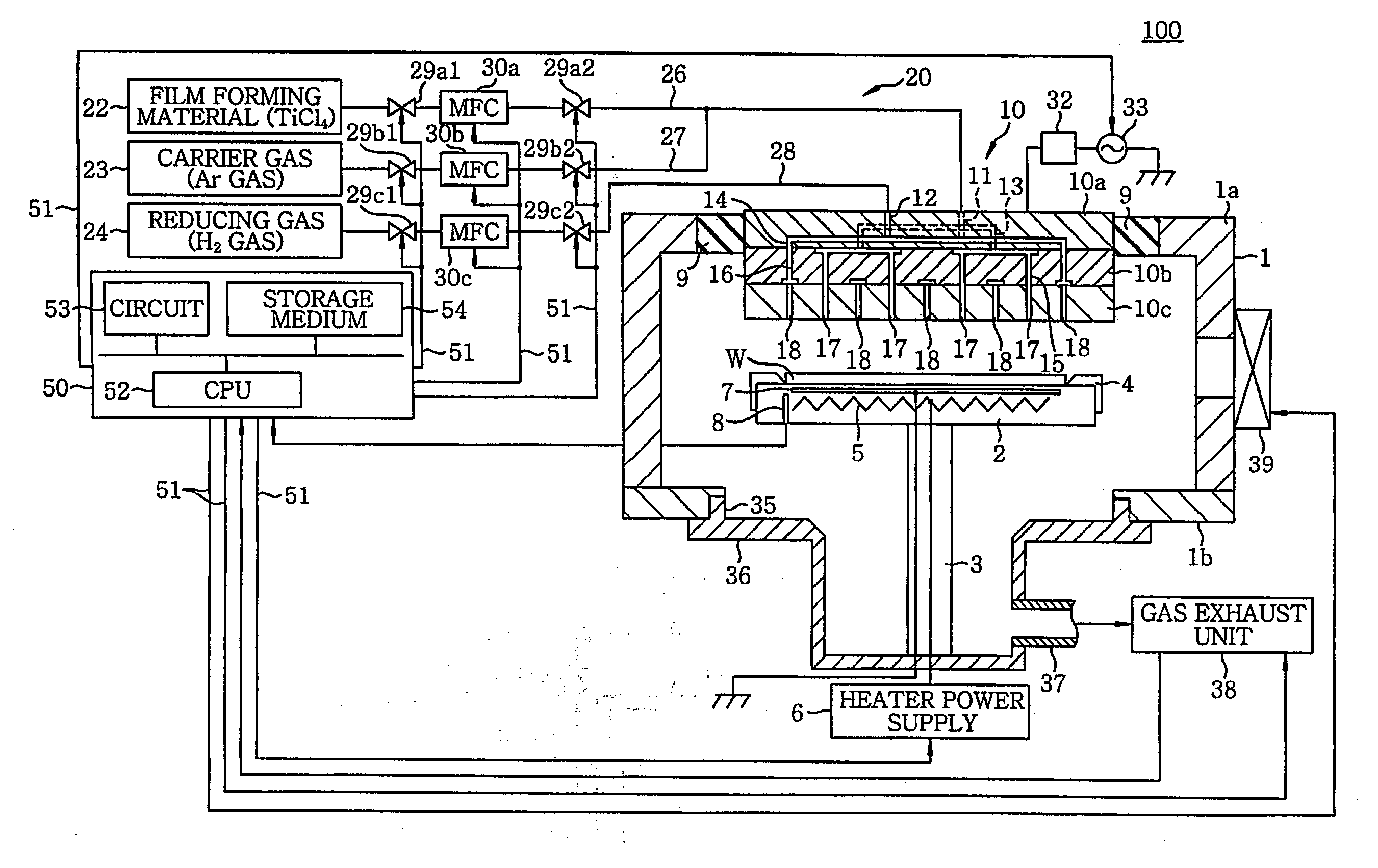
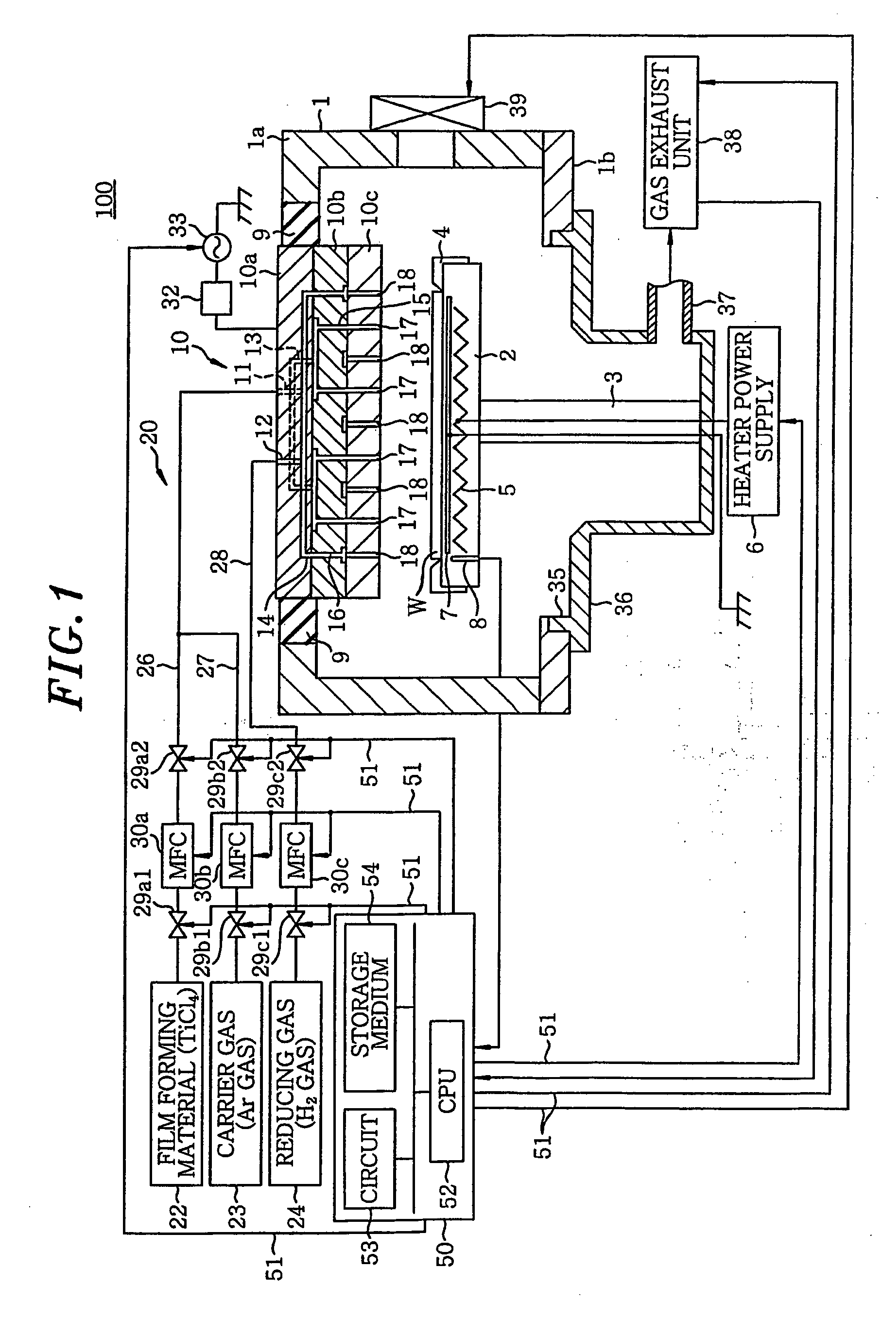
[0035] As shown in FIG. 1, each functional component of the film forming apparatus 100 in accordance with a preferred embodiment of the present invention is connected to a control computer 50 for automatically controlling an operation of the whole film forming apparatus via signal lines 51. Here, the functional components refer to all components operating to provide a predetermined film forming process condition to the film forming apparatus 100, including a heater power supply 6, valves 29a1 to 29c2, mass flow controllers (MFC's) 30a to 30c, a high frequency power supply 33, a gas exhaust unit 38, a gate valve 39, and other peripheral units. Herein, only a part of a plurality of signal lines 51 is shown for convenience. The control computer 50 is typically a general purpose computer capable of implementing various functions based on executable so...


PUM


Abstract

A film forming method is provided for forming a thin film including a metal on a substrate by alternately supplying the substrate with a film forming material including the metal and a reducing gas. At least a part of the film forming material is dissociated or decomposed in vapor phase by plasma and supplied onto the substrate.

Description

[0001] This application is a Continuation-In-Part Application of PCT International Application No. PCT / JP2005 / 003340 filed on Feb. 28, 2005, which designated the United States.FIELD OF THE INVENTION [0002] The present invention relates to a method for forming a thin film containing a metal, such as a metal film and a metal nitride film; and, more particularly, to a process of forming a metal nitride film or a metal film used for a semiconductor device circuit. BACKGROUND OF THE INVENTION [0003] In a wiring process of a semiconductor integrated circuit, a formation of a barrier film is necessary to suppress a Cu film from diffusing into a low dielectric interlayer insulating film (low-K film). As for the barrier film, TiN, TaN, WN, Ti, Ta, W and the like are considered to be promising materials therefor. [0004] S. M. Rossnagel et al, in “Plasma-enhanced Atomic Layer Deposition of Ta and Ti for Interconnect Diffusion Barriers,” J. VacSci. Technol. B 18(4), July / August 2000, disclose a...

Claims


Application Information

Patent Timeline
IPC IPC(8): H01L21/00G06F19/00C23C16/00H01L21/20C23C16/455C23C16/515H01L21/28H01L21/285H01L21/768
CPCC23C16/45542H01L21/76841H01L21/28562C23C16/515C23C16/45553C23C16/4408
Inventor YOSHII, NAOKIKOJIMA, YASUHIKO
Owner TOKYO ELECTRON LTD
Why Eureka
Try Eureka