Organic light emitting device

Inactive Publication Date: 2013-07-18
ELECTRONICS & TELECOMM RES INST
View PDF6 Cites 31 Cited by
  • Summary
  • Abstract
  • Description
  • Claims
  • Application Information

AI Technical Summary

Benefits of technology

[0012]The present invention provides an organic light emitting device having high

Problems solved by technology

However, since a transparent substrate used for organic light emitting devices, for example, a glass substrate, has a low refractive index of about 1.5, some limitations in the light extraction may occur.
However, since the refractive index of ITO typically used as an anod

Method used


Image

  • Organic light emitting device
  • Organic light emitting device
  • Organic light emitting device

Examples


Embodiment Construction

[0038]Preferred embodiments of the present invention will be described below in more detail with reference to the accompanying drawings. The present invention may, however, be embodied in different forms and should not be constructed as limited to the embodiments set forth herein. Rather, these embodiments are provided so that this disclosure will be thorough and complete, and will fully convey the scope of the present invention to those skilled in the art.

[0039]Hereinafter, it will be described about an exemplary embodiment of the present invention in conjunction with the accompanying drawings.

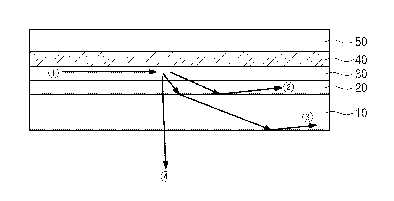
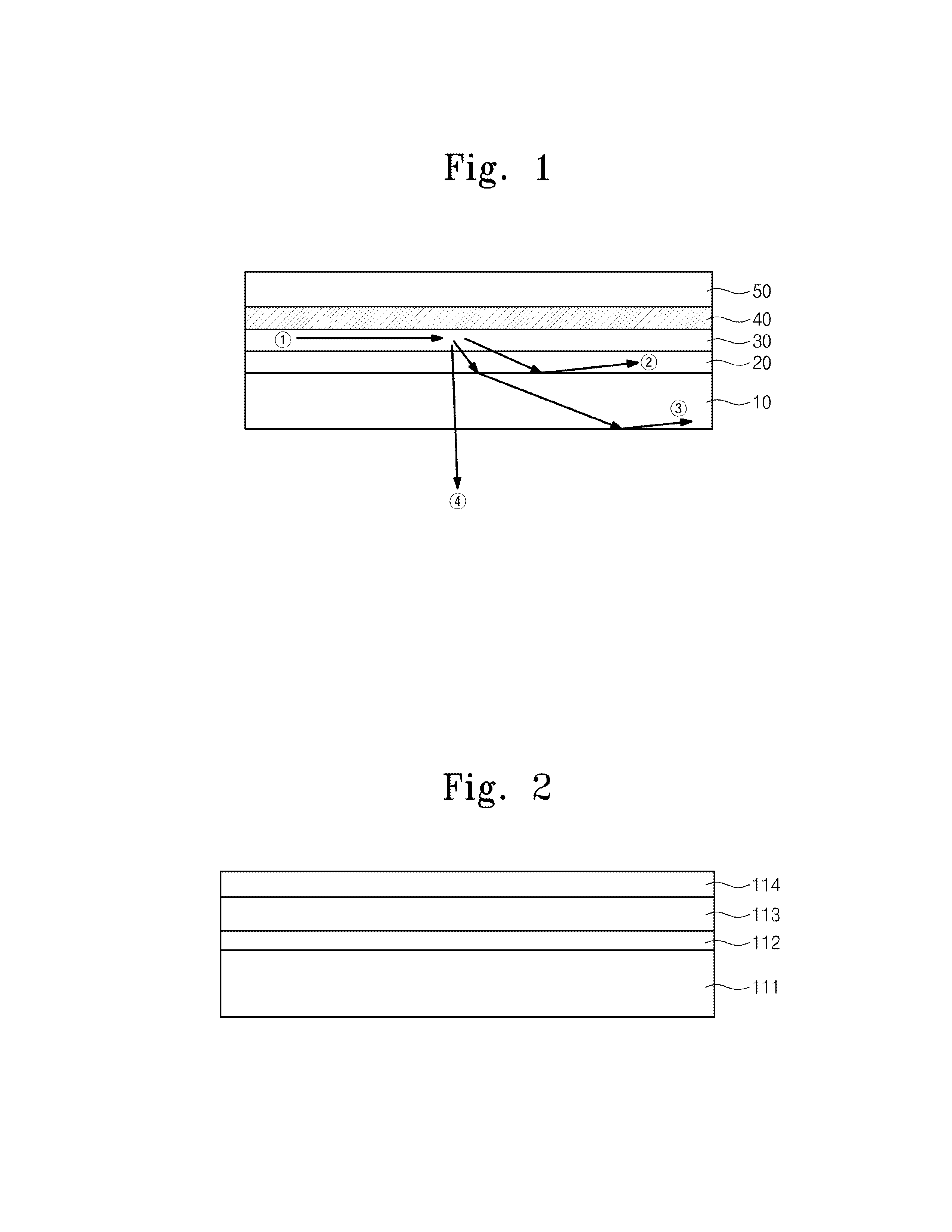
[0040]FIG. 2 is a schematic view illustrating an organic light emitting device according to an embodiment of the present invention.

[0041]The organic light emitting device of FIG. 2 includes a substrate 111, a first electrode 112, an organic light emitting layer 113, and a second electrode 114, which are sequentially stacked.

[0042]The substrate 111 provides a mechanical strength to the organic...


PUM


Abstract

Provided is an organic light emitting device. The organic light emitting device includes: a first electrode on a substrate, a second electrode on the first electrode, an organic light emitting layer between the first electrode and the second electrode, an embossing layer between the first electrode and the substrate and a planarization layer between the first electrode and the embossing layer.

Description

CROSS-REFERENCE TO RELATED APPLICATIONS[0001]This U.S. non-provisional patent application claims priority under 35 U.S.C. §119 of Korean Patent Application No. 10-2012-0005620, filed on Jan. 18, 2012, the entire contents of which are hereby incorporated by reference.BACKGROUND OF THE INVENTION[0002]The present invention disclosed herein relates to an organic light emitting device, and more particularly, to an organic light emitting device having high light extraction efficiency, lowering leakage current, and improving reliability.[0003]An organic light emitting device, for example, an organic light emitting diode is a light emitting device, where excitons occur when holes supplied from an anode electrode and electrons supplied from a cathode electrode are combined in an organic light emitting layer therebetween and they are recombined again. The organic light emitting diode as a self-light-emitting device is applied to a display device and developed due to its wide viewing angle, fa...

Claims


Application Information

Patent Timeline
IPC IPC(8): H01L51/52
CPCH01L51/5203H01L51/5268H10K50/854H10K50/13H10K50/852H10K50/805
Inventor CHO, DOO-HEESHIN, JIN WOOKLEE, JEONG IKCHU, HYE YONGHAN, JUN-HANHWANG, JOO HYUNPARK, SEUNG KOOMOON, JAEHYUNCHO, NAM SUNGHUH, JIN WOOJOO, CHUL WOONG
Owner ELECTRONICS & TELECOMM RES INST
Why Eureka
Try Eureka