Gate driving circuit and display apparatus having the same

a driving circuit and display device technology, applied in the direction of oscillator generators, digital storage, pulse techniques, etc., can solve the problems of shortening the lifetime deteriorating the reliability of the gate driving circui

Active Publication Date: 2013-07-18
SAMSUNG DISPLAY CO LTD
View PDF0 Cites 35 Cited by
  • Summary
  • Abstract
  • Description
  • Claims
  • Application Information

AI Technical Summary

Benefits of technology

[0007]In an exemplary embodiment of a gate driving circuit according to the present invention, the N-th stage of the gate driving circuit includes a pull-up control part, a pull-up part, a carry part, a first pull-down part and a second pull-down part. The pull-up control part applies a previous carry signal to a first node from a stage previous to the N-th stage in response to the previous carry signal. The pull-up part outputs an N-th gate output signal based on a clock signal in response to a signal applied to the first node. The carry part outputs an N-th carry signal based on the clock signal in response to the signal applied to the first node. The first pull-down part includes a plurality of transistors connected to each other in series. The first pull-down part pulls down a signal at the first node to a second off voltage in response to a next carry signal from a stage after the N-th stage. The second pull-down part pulls down the N-th gate output signal to a first off voltage in response to the next carry signal. N is a natural number.
[0008]In an exemplary embodiment of a gate driving circuit according to the present invention, the N-th stage of the gate driving circuit includes a pull-up control part, a pull-up part, a carry part, a first pull-down part, a second pull-down part, an inverting part. The pull-up control part applies a previous carry signal to a first node from a stage previous to the N-th stage in response to the previous carry signal. The pull-up part outputs an N-th gate output signal based on a clock signal in response to a signal applied to the first node. The carry part outputs an N-th carry signal based on the clock signal in response to the signal applied to the first node. The first pull-down part pulls down a signal at the first node to a second off voltage in response to a next carry signal from a stage after the N-th stage. The second pull-down part pulls down the N-th gate output signal to a first off voltage in response to the next carry signal. The inverting part is configured to receive the clock signal and the second off voltage, and output an inverting signal. The inverting part of the N-th stage is connected to an inverting part of at least one stage that is after the N-th stage. N is a natural number.
[0009]In an exemplary embodiment of a display apparatus according to the present invention, the display apparatus includes a display panel, a data driving circuit and a gate driving circuit. The display panel has a display region on which an image is displayed and a peripheral region adjacent the display region. The data driving circuit applies a data voltage to the display panel. The gate driving circuit applies a gate output signal to the display panel. An N-th stage of the gate driving circuit includes a pull-up control part, a pull-up part, a carry part, a first pull-down part and a second pull-down part. The pull-up control part applies a previous carry signal to a first node from a stage previous to the N-th stage in response to the previous carry signal. The pull-up part outputs an N-th gate output signal based on a clock signal in response to a signal applied to the first node. The carry part outputs an N-th carry signal based on the clock signal in response to the signal applied to the first node. The first pull-down part includes a plurality of transistors connected to each other in series. The first pull-down part pulls down a signal at the first node to a second off voltage in response to a next carry signal from a stage after the N-th stage. The second pull-down part pulls down the N-th gate output signal to a first off voltage in response to the next carry signal. N is a natural number.
[0010]In an exemplary embodiment of a display apparatus according to the present invention, the display apparatus includes a display panel, a data driving circuit and a gate driving circuit. The display panel has a display region on which an image is displayed and a peripheral region adjacent the display region. The data driving circuit applies a data voltage to the display panel. The gate driving circuit applies a gate output signal to the display panel. An N-th stage of the gate driving circuit includes a pull-up control part, a pull-up part, a carry part, a first pull-down part, a second pull-down part, an inverting part. The pull-up control part applies a previous carry signal to a first node from a stage previous the N-th stage in response to the previous carry signal. The pull-up part outputs an N-th gate output signal based on a clock signal in response to a signal applied to the first node. The carry part outputs an N-th carry signal based on the clock signal in response to the signal applied to the first node. The first pull-down part pulls down a signal at the first node to a second off voltage in response to a next carry signal from a stage after the N-th stage. The second pull-down part pulls down the N-th gate output signal to a first off voltage in response to the next carry signal. The inverting part of the N-th stage is configured to receive the clock signal and the second off voltage, and output an inverting signal. The inverting part of the N-th stage is connected to an inverting part of at least one stage that is after the N-th stage. N is a natural number.
[0011]A gate driving circuit according to an exemplary embodiment of the invention includes first through sixth stages. Each of the second and fourth stages includes a pull-up control part, a charging part, a pull-up part, a carry part, an inverting part, a first pull-down part, a second pull-down part, a first holding part, a second holding part, a third holding part, and a reset part. A clock signal is applied to each inverting part and each carry part. A first carry signal output from the first stage is applied to the pull-up control part of the second stage. The second stage outputs a second carry signal. A third carry signal output from the third stage is applied to the first pull-down part of the second stage, the second pull-down part of the second stage, and the pull-up control part of the fourth stage, wherein a fourth carry signal output from the fourth stage is applied to the reset part of the second stage. A fifth carry signal output from the fifth stage is applied to the first pull-down part and the second pull-down part of the fourth stage. A sixth carry signal output from the sixth stage is applied to the reset part of the fourth stage.

Problems solved by technology

When a relatively high voltage is applied between a drain electrode and a source electrode of a switching element in the gate driving circuit, a reliability of the gate driving circuit may deteriorate and a lifetime of the gate driving circuit may shorten.

Method used


Image

  • Gate driving circuit and display apparatus having the same
  • Gate driving circuit and display apparatus having the same
  • Gate driving circuit and display apparatus having the same

Examples


Embodiment Construction

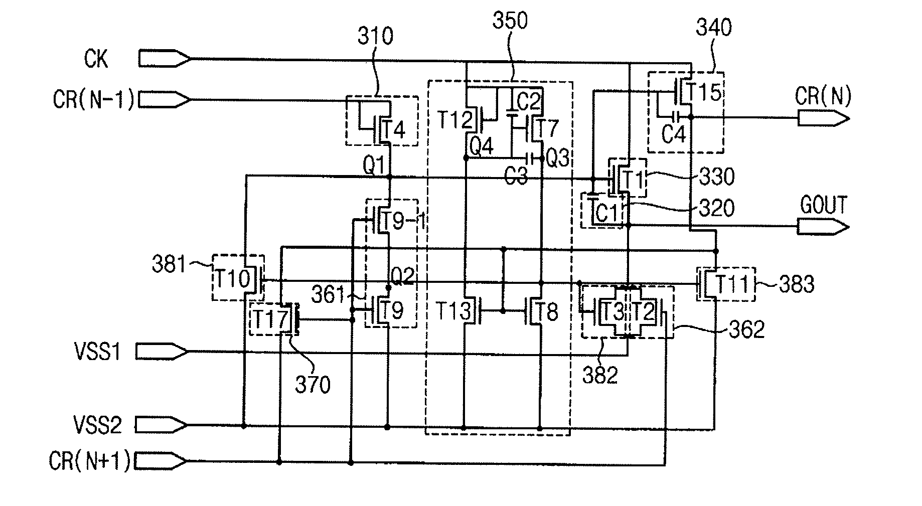
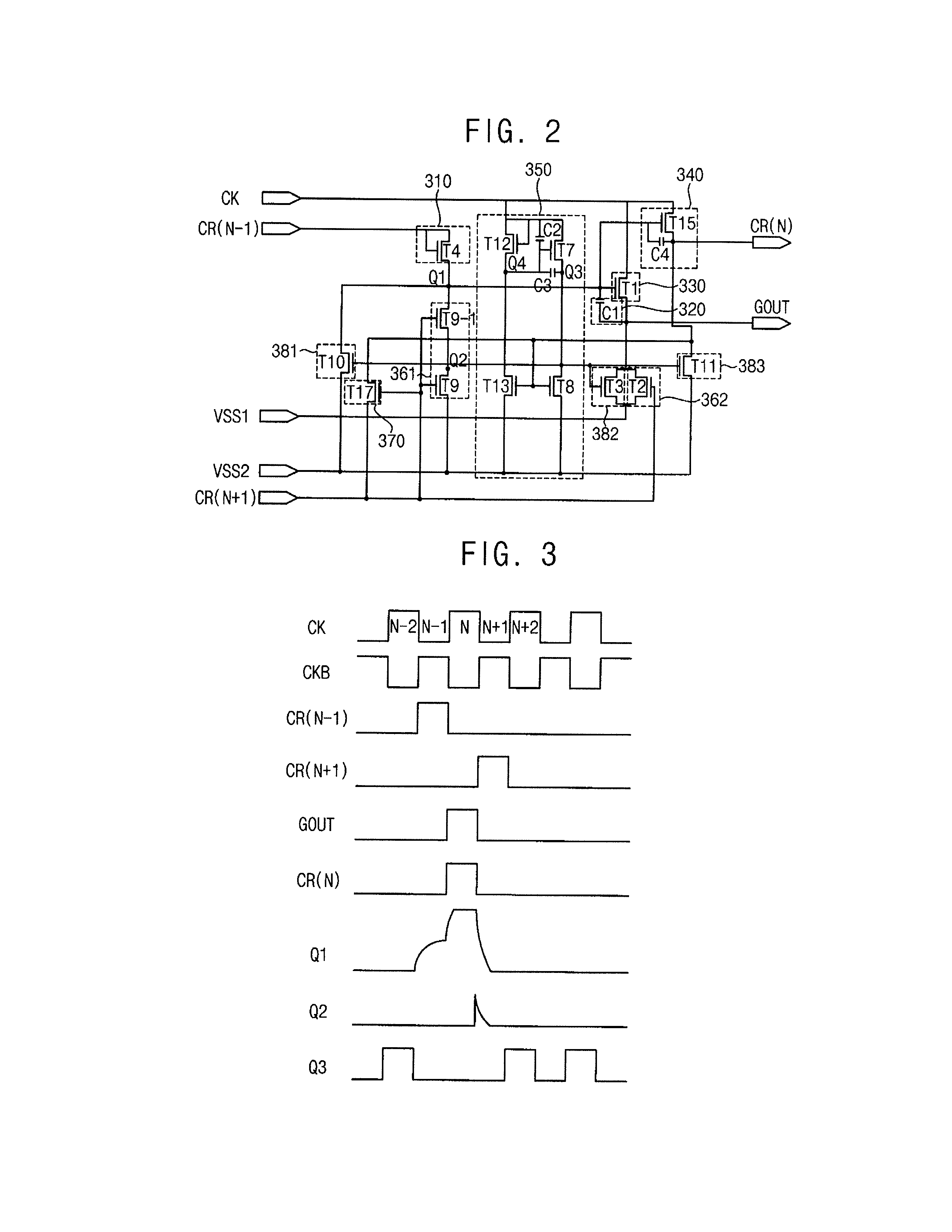
[0020]Hereinafter, the present invention will be explained in detail with reference to the accompanying drawings, in exemplary embodiments thereof are shown. The described embodiments may be modified in various different ways, without departing from the spirit or scope of the disclosure. As used herein, the singular forms, “a,”“an” and “the” are intended to include the plural forms as well, unless the context clearly indicates otherwise.

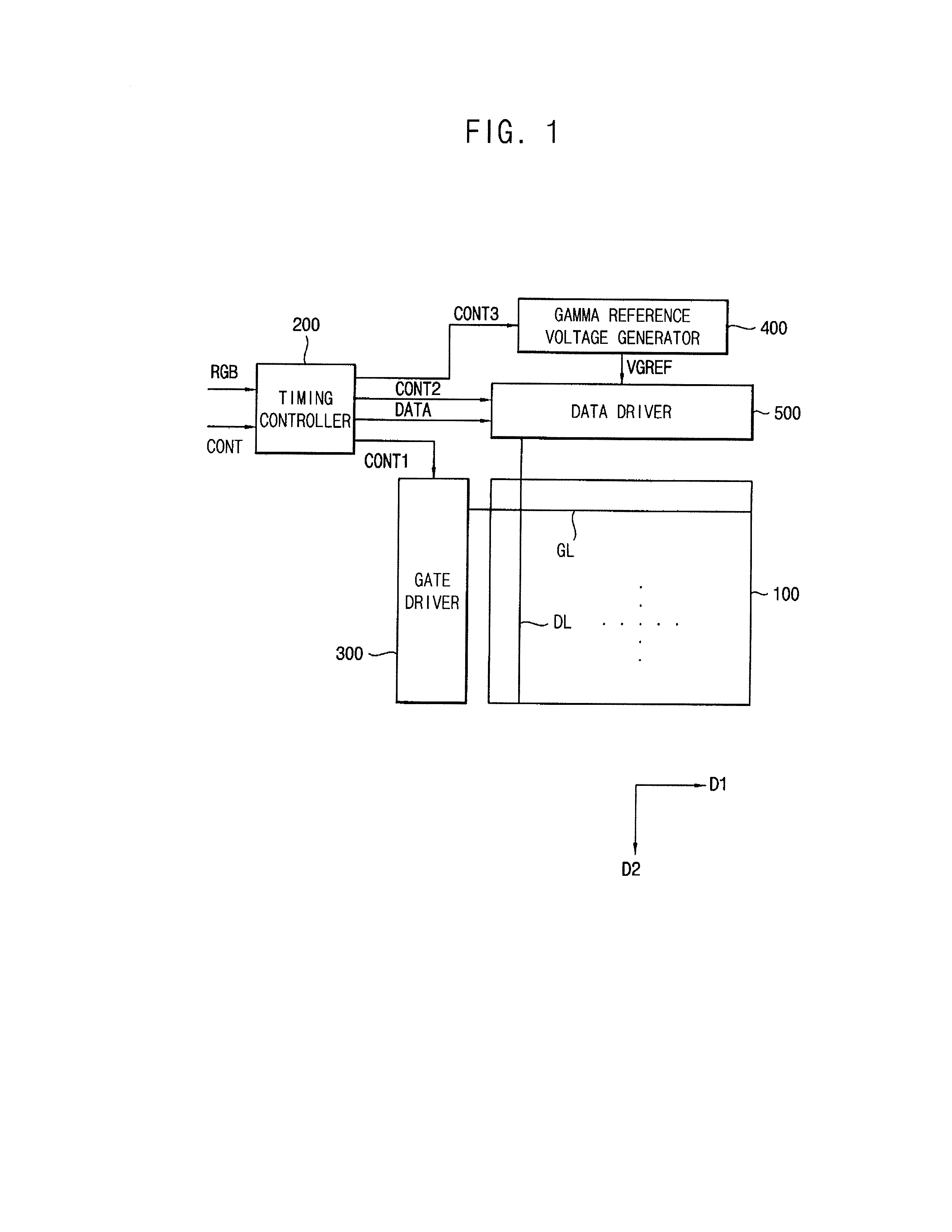
[0021]FIG. 1 is a block diagram illustrating a display apparatus according to an exemplary embodiment of the present invention.

[0022]Referring to FIG. 1, the display apparatus includes a display panel 100 and a panel driver. The panel driver includes a timing controller 200, a gate driver 300, a gamma reference voltage generator 400 and a data driver 500.

[0023]The display panel 100 has a display region that is configured to display an image and a peripheral region adjacent the display region. In an exemplary embodiment, images are not displayed withi...


PUM


Abstract

A gate driving circuit includes a pull-up control part, a pull-up part, a carry part, a first pull-down part and a second pull-down part. The pull-up control part applies a carry signal from a previous stage to a first node. The pull-up part outputs an N-th gate output signal based on a clock signal. The carry part outputs an N-th carry signal based on the clock signal in response to the signal applied to the first node. The first pull-down part includes a plurality of transistors connected to each other in series. The first pull-down part pulls down a signal at the first node to a second off voltage in response to a carry signal of a next stage. The second pull-down part pulls down the N-th gate output signal to a first off voltage in response to the carry signal of the next stage.

Description

PRIORITY STATEMENT[0001]This application claims priority under 35 U.S.C. §119 to Korean Patent Application No. 10-2012-0003723, filed on Jan. 12, 2012 in the Korean Intellectual Property Office KIPO, the disclosure of which is incorporated by reference in its entirety herein.TECHNICAL FIELD[0002]Exemplary embodiments of the present invention relate to a gate driving circuit and a display apparatus having the display panel.DISCUSSION OF RELATED ART[0003]A liquid crystal display (“LCD”) apparatus may include a first substrate having a pixel electrode, a second substrate having a common electrode and a liquid crystal layer disposed between the first and second substrate. An electric field is generated by voltages applied to the pixel electrode and the common electrode. By adjusting an intensity of the electric field, a transmittance of a light passing through the liquid crystal layer may be adjusted so that a desired image may be displayed.[0004]A display apparatus may include a displa...

Claims


Application Information

Patent Timeline
Patent Type & Authority Applications(United States)
IPC IPC(8): H03K3/00
CPCG11C19/184G11C19/28H03K3/012G09G2310/0286G09G2330/021G09G3/3674G09G3/36
Inventor YOON, SOO-WANKWON, YEONG-KEUNKIM, JI-SUNYOON, YOUNG-SOOCHAI, CHONG-CHUL
Owner SAMSUNG DISPLAY CO LTD
Why Eureka
Try Eureka