
Replacement source/drain finfet fabrication

Active Publication Date: 2013-07-25
ADVANCED ION BEAM TECHNOLOGY INC
View PDF6 Cites 32 Cited by
  • Summary
  • Abstract
  • Description
  • Claims
  • Application Information

AI Technical Summary

Benefits of technology

The patent text describes a process for making a finFET (which is a type of semiconductor device) by etching a fin on a semiconductor wafer and then adding a gate stack with an insulating layer and a conductive gate material. Dopants are then added to the source and drain regions, which are the parts of the fin that will be used to create the device. The technical effect of this process is to create a more efficient and reliable finFET semiconductor device.

Problems solved by technology

However, the non-planar nature of finFETs may lead to several difficulties during fabrication.
To overcome shadowing effects from nearby finFETs, the implant may need to be performed at multiple angles or orientations, which may increase implanter tool complexity, implanting cost, and processing time.
However, using design rules to increase structure spacing will result in less dense circuits.
However, plasma doping may have its own set of disadvantages, such as doping control and limits on doping concentrations.

Method used


Image

  • Replacement source/drain finfet fabrication
  • Replacement source/drain finfet fabrication
  • Replacement source/drain finfet fabrication

Examples


Embodiment Construction

[0029]The following description is presented to enable a person of ordinary skill in the art to make and use the various embodiments. Descriptions of specific devices, techniques, and applications are provided only as examples. Various modifications to the examples described herein will be readily apparent to those of ordinary skill in the art, and the general principles defined herein may be applied to other examples and applications without departing from the spirit and scope of the various embodiments. Thus, the various embodiments are not intended to be limited to the examples described herein and shown, but are to be accorded the scope consistent with the claims.

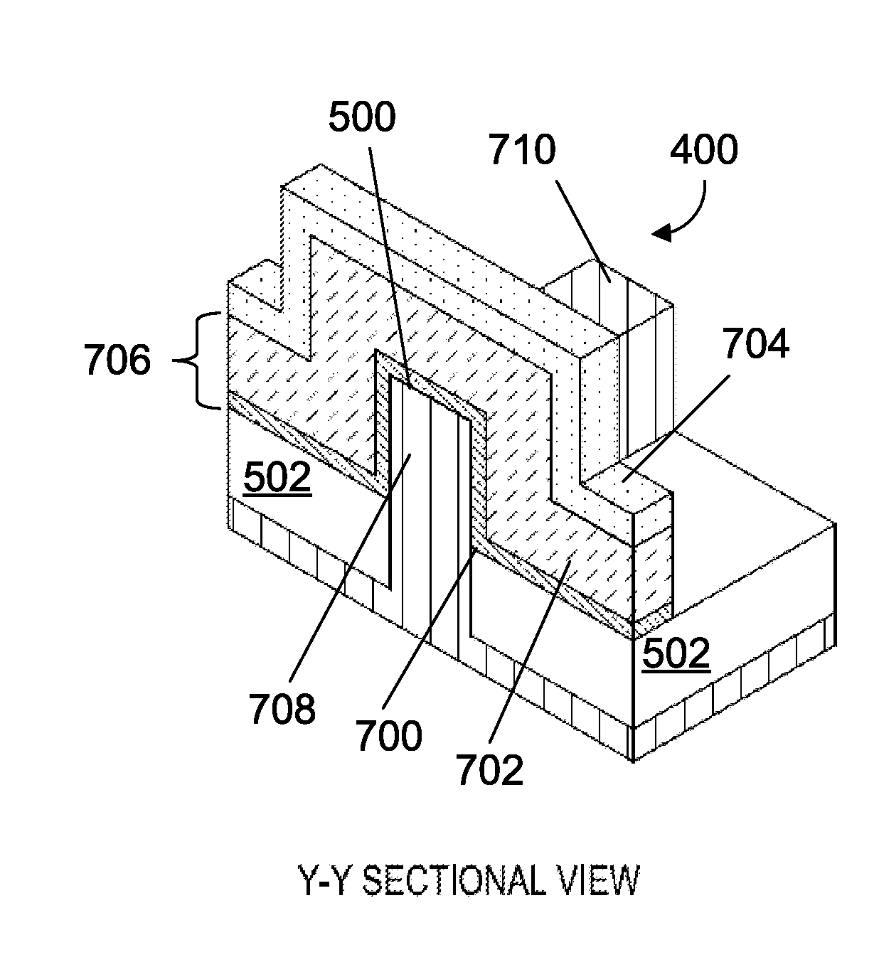
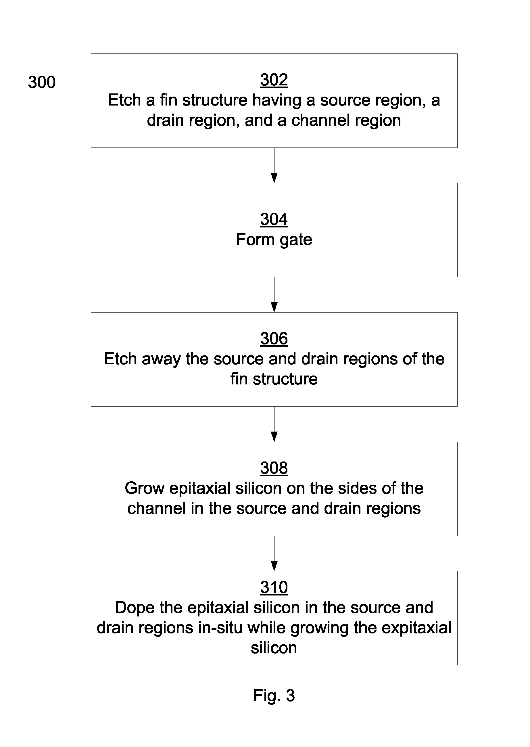
[0030]FIG. 3 depicts an exemplary process 300 for fabricating a finFET. Corresponding FIGS. 4A-4C; 5A-5C; 6A-6C; 7A-7C; 8A-8C; 9A-9C; and 10A-10C depict the finFET at various stages of fabrication according to exemplary process 300 (FIG. 3).

[0031]In particular, FIGS. 4A-4C depict substrate 400, which is a portion of a s...


PUM


Abstract

A finFET is formed having a fin with a source region, a drain region, and a channel region between the source and drain regions. The fin is etched on a semiconductor wafer. A gate stack is formed having an insulating layer in direct contact with the channel region and a conductive gate material in direct contact with the insulating layer. The source and drain regions are etched to expose a first region of the fin. A portion of the first region is then doped with a dopant.

Description

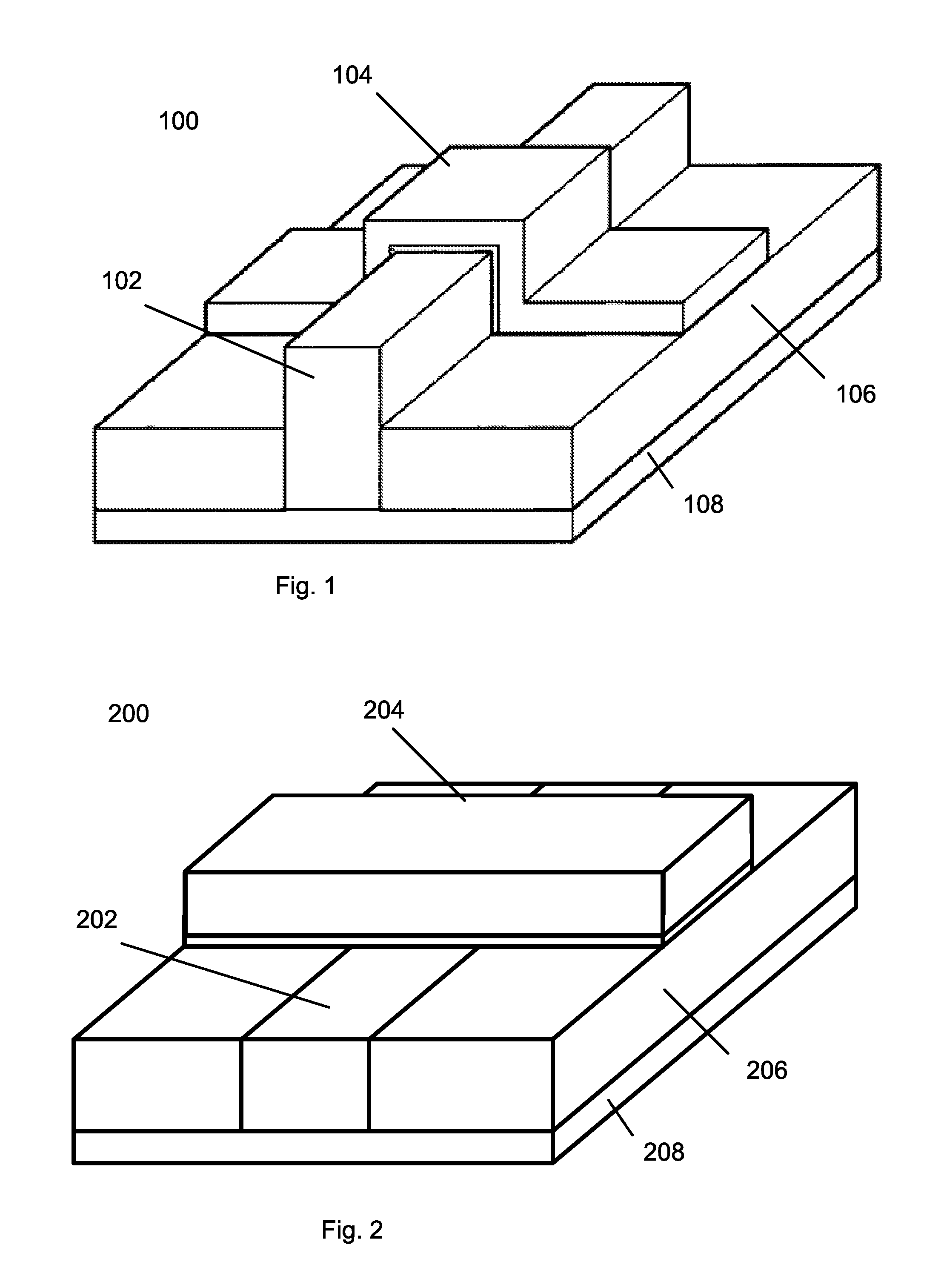
CROSS-REFERENCE TO RELATED APPLICATION[0001]This application is a continuation-in-part of U.S. patent application Ser. No. 13 / 192,378, filed Jul. 27, 2011, which is incorporated herein by this reference in its entirety.BACKGROUND[0002]1. Field[0003]The present disclosure relates generally to fabricating fin field effect transistors (finFETs), and, more specifically, to fabricating finFETs with replacement sources and drains.[0004]2. Description of Related Art[0005]A finFET is a non-planar multi-gate transistor that operates on the same principles as traditional metal oxide semiconductor field effect transistors (MOSFETs). An island or fin of silicon is first patterned on to the wafer. After forming the fin, a gate stack is deposited and patterned so that the patterned gate material runs perpendicular to the fin. Where the patterned gate material overlaps the fin, a gate for the finFET is formed. The finFET will have one gate on both vertical sidewalls of the fin. Depending on the si...

Claims


Application Information

Patent Timeline
IPC IPC(8): H01L29/66H01L29/78
CPCH01L29/66795H01L29/78684H01L21/02636H01L29/785H01L29/0673H01L29/66803
Inventor TANG, DANIELYEN, TZU-SHIH
Owner ADVANCED ION BEAM TECHNOLOGY INC
Learn More