

Ink jet print head with piezoelectric actuator
- Summary
- Abstract
- Description
- Claims
- Application Information
AI Technical Summary
Benefits of technology
Problems solved by technology
Method used
Image

Examples
first embodiment
[0053]Table 1 shows three examples of layer thicknesses of the first embodiment which satisfy the above formula.
TABLE 1Layer ThicknessLayer ThicknessLayer Thickness(nm)(nm)(nm)LayerExample 1Example 2Example 3TiW230150110PZT300020002000Pt300200100Ti303030SiO2500500500Si500050005000SiO2500500500
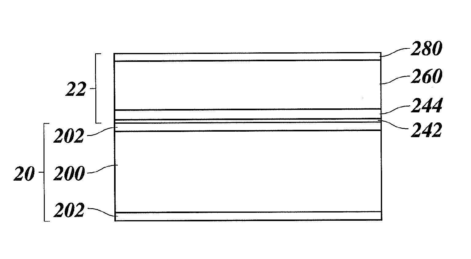
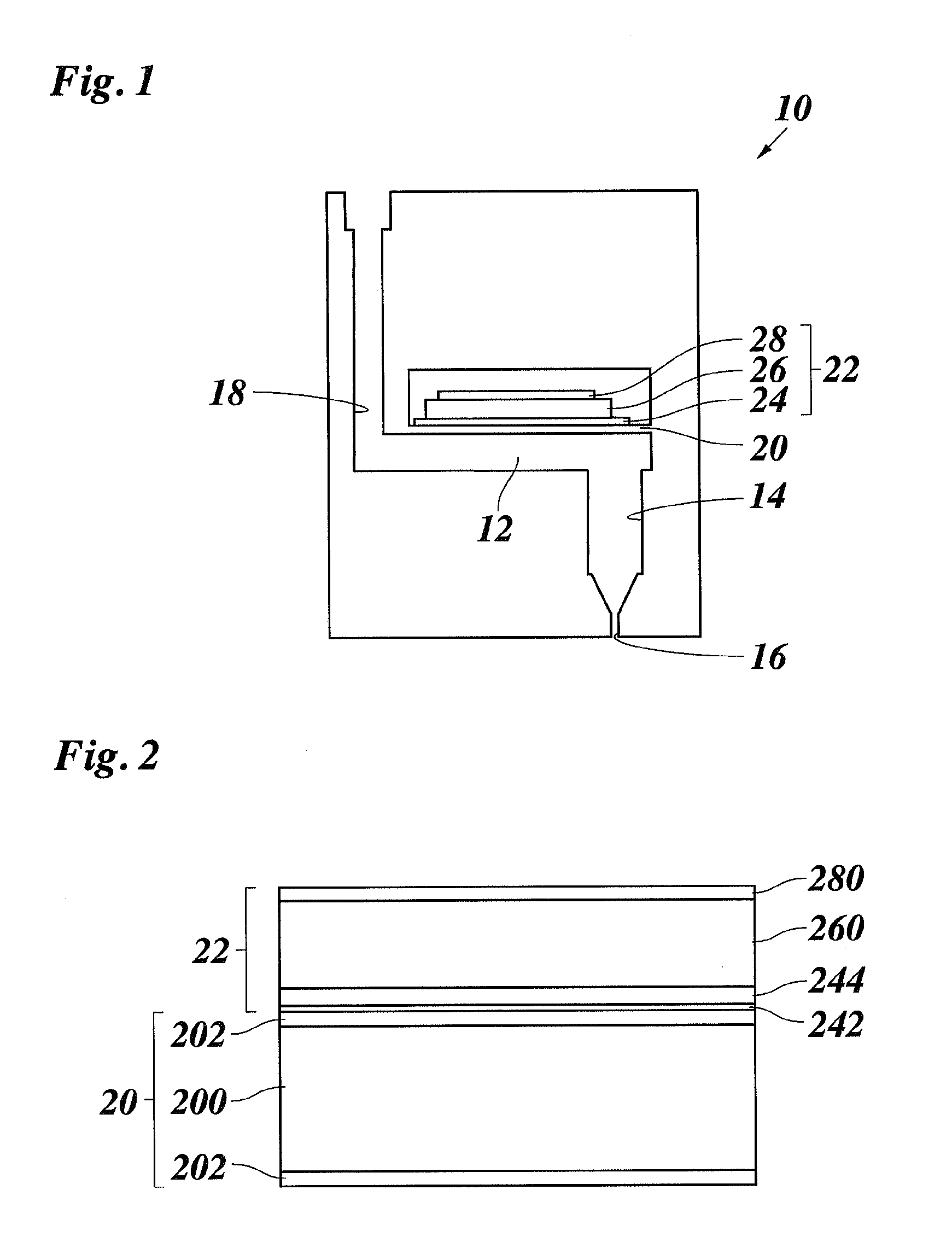
[0054]In the examples, the silicon layer 200 of the silicon substrate 20 has a thickness of 5000 nanometer, and the surface oxide layers 202 have a thickness of 500 nanometer each.
[0055]With a Pt layer 244 of 300 nanometer and a PZT layer 260 of 3000 nanometer, a TiW layer 280 having a thickness of 230 nanometer is expected to have a compressive stress that leads to a flatness of the multilayer package and, thus, the substrate 20.
[0056]With a PZT layer of 2000 nanometer, a TiW layer of 150 nanometer is sufficient for a lower electrode having a Pt layer of 200 nanometer, and a TiW layer of 110 nanometer is sufficient for a lower electrode Pt layer of 100 nanometer. Thus, the upper electrode TiW ...
second embodiment
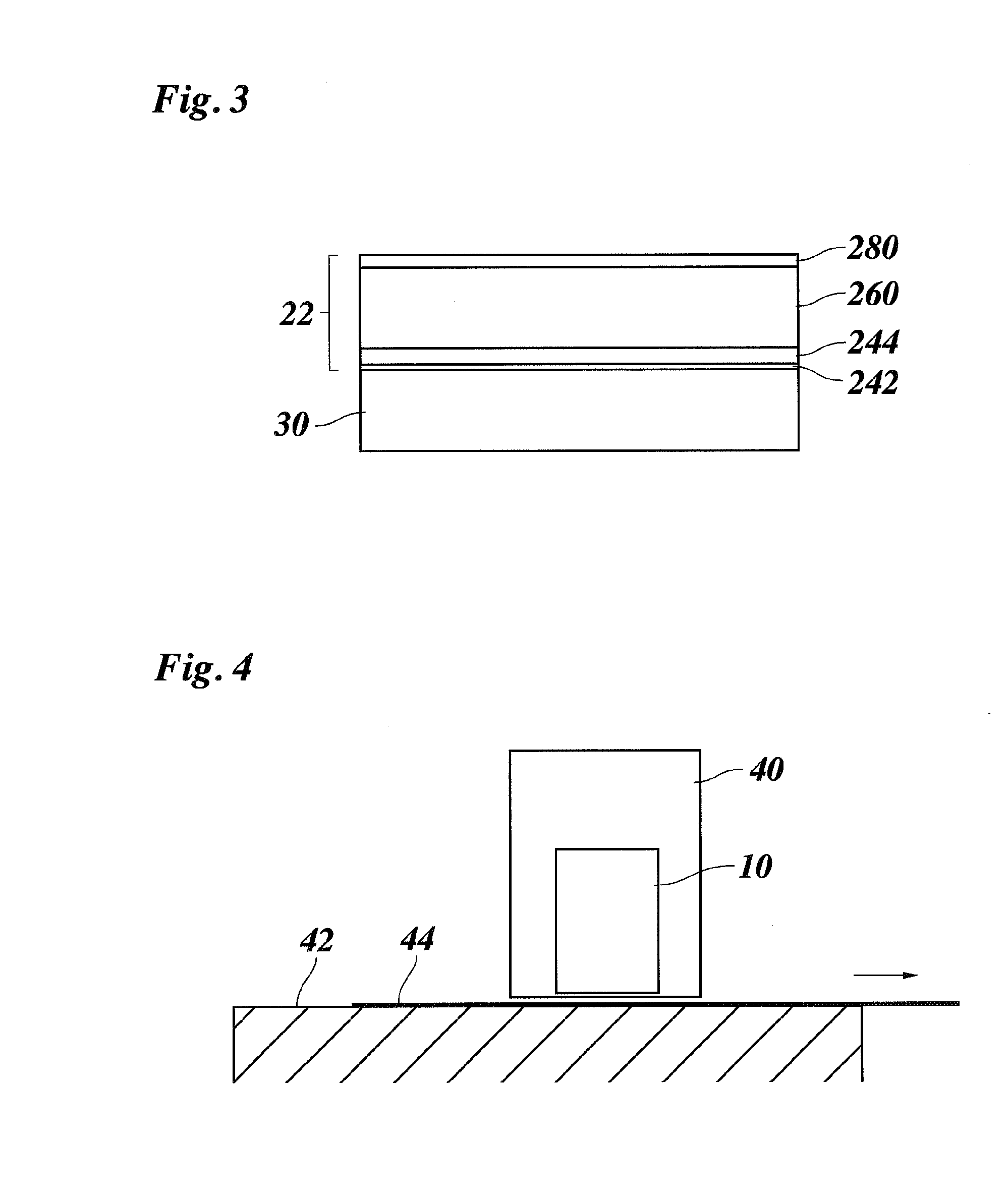
[0057]FIG. 3 shows an actuator membrane in the form of a multilayer package of a second embodiment having a silicon nitride (Si3N4) substrate 30. The substrate 30 and the piezoelectric actuator 22 form a multilayer package consisting of the Si3N4 layer of the substrate 30, an adhesion layer 242 of Titanium, a platinum layer 244, a PZT layer 280 and a TiW layer 280.
[0058]The layers may be prepared similar to the embodiment of FIG. 2. The piezoelectric actuator comprises the Ti adhesion layer 242 and the Pt layer 244 of the lower electrode 24, the piezoelectric layer 26 consisting of the PZT layer 260 and the upper electrode consisting of the Titanium-Tungsten film 280.
[0059]Table 2 shows layer thicknesses of two examples of the second embodiment.
TABLE 2Layer thickness (nm)Layer thickness (nm)LayerExample 1Example 2TiW85100PZT10002000Pt100100Ti3030Si3N410001000
[0060]For example, the substrate 30 has a thickness of 1000 nanometer. The adhesion layer 242 has a thickness of 30 nanometer,...
PUM
 Abstract
Description
Claims
Application Information