Bipolar multistate nonvolatile memory

a nonvolatile memory, bipolar technology, applied in the direction of negative resistance effect devices, bulk negative resistance devices, semiconductor devices, etc., can solve the problems of increasing cost and complexity, posing challenges to traditional nonvolatile memory technology, etc., to reduce the vertical or horizontal physical density requirements necessary, reduce the complexity of the manufacturing process of nonvolatile memory devices, the effect of reducing the complexity of the vertical or horizontal physical density

Active Publication Date: 2013-08-15
INTERMOLECULAR
View PDF1 Cites 58 Cited by
  • Summary
  • Abstract
  • Description
  • Claims
  • Application Information

AI Technical Summary

Benefits of technology

[0009]Embodiments of the invention generally relate to a resistive switching nonvolatile memory device having multiple layers of variable resistance switching material within a resistive switching memory element that are configured to increase the number of logic states to be greater than two per memory element. The resistive switching memory element may have any suitable number of variable resistance switching layers (hereafter variable resistance layers). If the memory element has a total of “n” variable resistance layers, where “n” is a positive integer, the resistive switching memory element may exhibit “n+1” stable states. The variable resistance layers each having different switching characteristics can be formed by varying the layers materials or material properties. The memory element device decreases the vertical or horizontal physical density requirements necessary to achieve the same nonvolatile storage capacity and reduces the complexity of the nonvolatile memory device manufacturing process.

Problems solved by technology

However, as device dimensions shrink, scaling issues are posing challenges for traditional nonvolatile memory technology.
However, the above methods may introduce additional cost and complexity.

Method used


Image

  • Bipolar multistate nonvolatile memory
  • Bipolar multistate nonvolatile memory
  • Bipolar multistate nonvolatile memory

Examples


Embodiment Construction

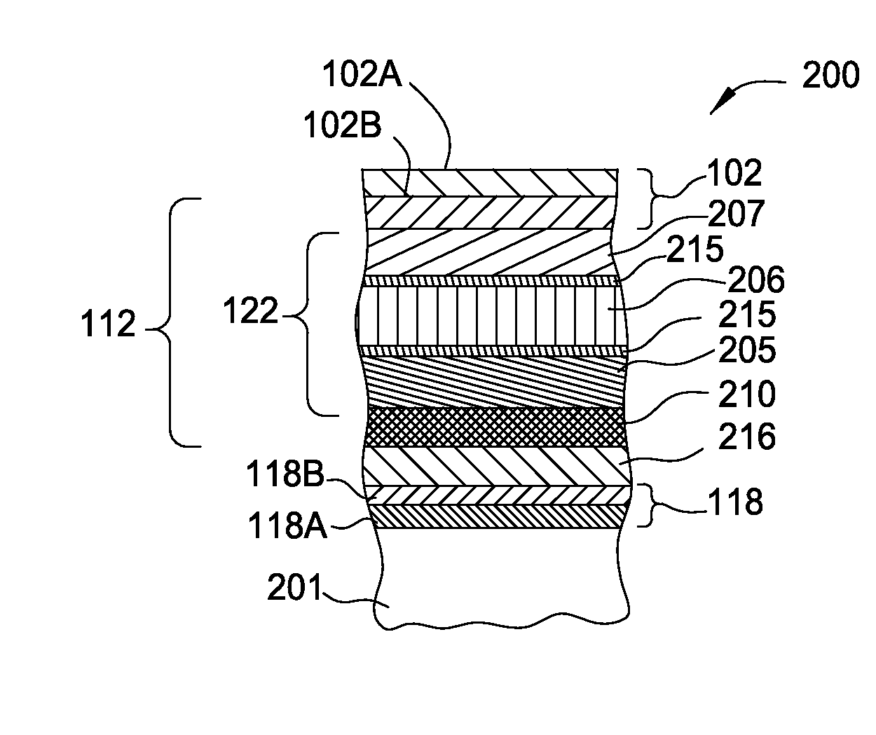
[0028]Embodiments of the invention generally include a method of forming a nonvolatile memory device that contains a resistive switching memory element that has multiple variable resistance layers. Each variable resistance layer may have at least an associated high resistance state and an associated low resistance state (e.g., two stable states). As the resistance of each variable resistance layer determines the digital data that is stored (e.g., logic “zero” or logic “one”), the multiple variable resistance layers per memory element allow for additional data storage without the need to further increase the size of the nonvolatile memory device and array of non-volatile memory devices that contain multiple memory elements.

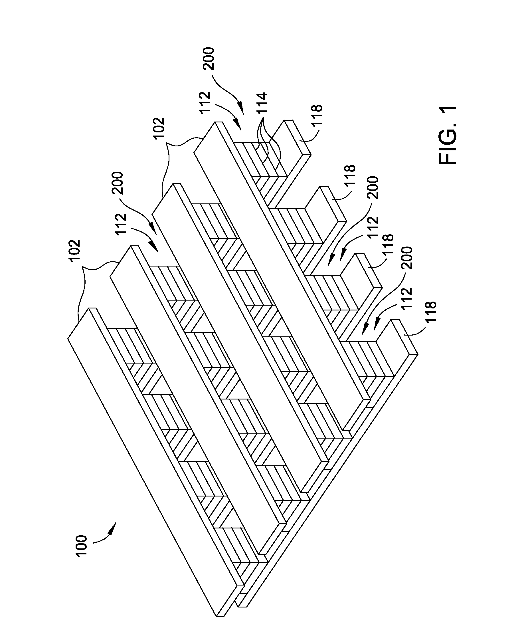
[0029]An illustrative memory array 100 of nonvolatile resistive switching memory devices 200 (hereafter switching memory device 200), which each generally include at least one resistive switching memory element 112, is illustrated in FIG. 1. Memory array 100 may be...


PUM


Abstract

Embodiments generally include a method of forming a nonvolatile memory device that contains a resistive switching memory element that has an improved device switching capacity by using multiple layers of variable resistance layers. In one embodiment, the resistive switching element comprises at least three layers of variable resistance materials to increase the number of logic states. Each variable resistance layer may have an associated high resistance state and an associated low resistance state. As the resistance of each variable resistance layer determines the digital data bit that is stored, the multiple variable resistance layers per memory element allows for additional data storage without the need to further increase the density of nonvolatile memory devices. Typically, resistive switching memory elements may be formed as part of a high-capacity nonvolatile memory integrated circuit, which can be used in various electronic devices, such as digital cameras, mobile telephones, handheld computers, and music players.

Description

BACKGROUND OF THE INVENTION[0001]1. Field of the Invention[0002]This invention relates to nonvolatile memory elements, and more particularly, to methods for forming resistive switching memory elements with multiple variable resistance layers.[0003]2. Description of the Related Art[0004]Nonvolatile memory elements are used in systems in which persistent storage is required. For example, digital cameras use nonvolatile memory cards to store images and digital music players use nonvolatile memory to store audio data. Nonvolatile memory is also used to persistently store data used by a computer.[0005]Nonvolatile memory is often formed using electrically-erasable programmable read only memory (EEPROM) technology. This type of nonvolatile memory contains floating gate transistors that can be selectively programmed or erased by application of suitable voltages to their terminals.[0006]As fabrication techniques improve, it is becoming possible to fabricate nonvolatile memory elements with i...

Claims


Application Information

Patent Timeline
Patent Type & Authority Applications(United States)
IPC IPC(8): H01L25/04H01L47/00
CPCH01L45/1253H01L45/145H01L45/147H01L45/1608H01L27/2481H01L45/1233H01L45/146H01L45/1616H01L27/2409H01L45/08H10B63/84H10B63/20H10N70/24H10N70/826H10N70/8833H10N70/023H10N70/021H10N70/841H10N70/883H10N70/8836
Inventor CHIANG, TONY P.
Owner INTERMOLECULAR
Why Eureka
Try Eureka