

Method of forming pattern
a pattern and pattern technology, applied in the field of pattern formation, can solve the problems of high production cost, increase the number of steps, and increase the complexity of steps, and achieve the effects of low production cost, simple process, and excellent uniformity
Active Publication Date: 2013-08-15
TOKYO OHKA KOGYO CO LTD +1
View PDF2 Cites 31 Cited by
- Summary
- Abstract
- Description
- Claims
- Application Information
AI Technical Summary
Benefits of technology
The present invention provides a method for forming a pattern that can produce fine patterns with uniformity. The method improves the line width roughness of a first pattern composed of a resist film, which helps in achieving uniformity of a second pattern. The method also uses a specific resist composition for forming the first pattern and has a simple process, low production cost, and improved productivity.
Problems solved by technology
However, when a double patterning process recited in non-Patent Documents 1 and 2 is applied, there is a problem that the number of steps is increased, and steps become complicated with high production cost, and productivity is decreased.
As a result, the SWT process is complicated.
Method used
View moreImage
Smart ImageViewing Examples

Examples
examples
[0621]As follows is a description of examples of the present invention, although the scope of the present invention is by no way limited by these examples.
Login to View More PUM
| Property | Measurement | Unit |
|---|---|---|
| temperature | aaaaa | aaaaa |
| temperature | aaaaa | aaaaa |
| temperature | aaaaa | aaaaa |
Abstract
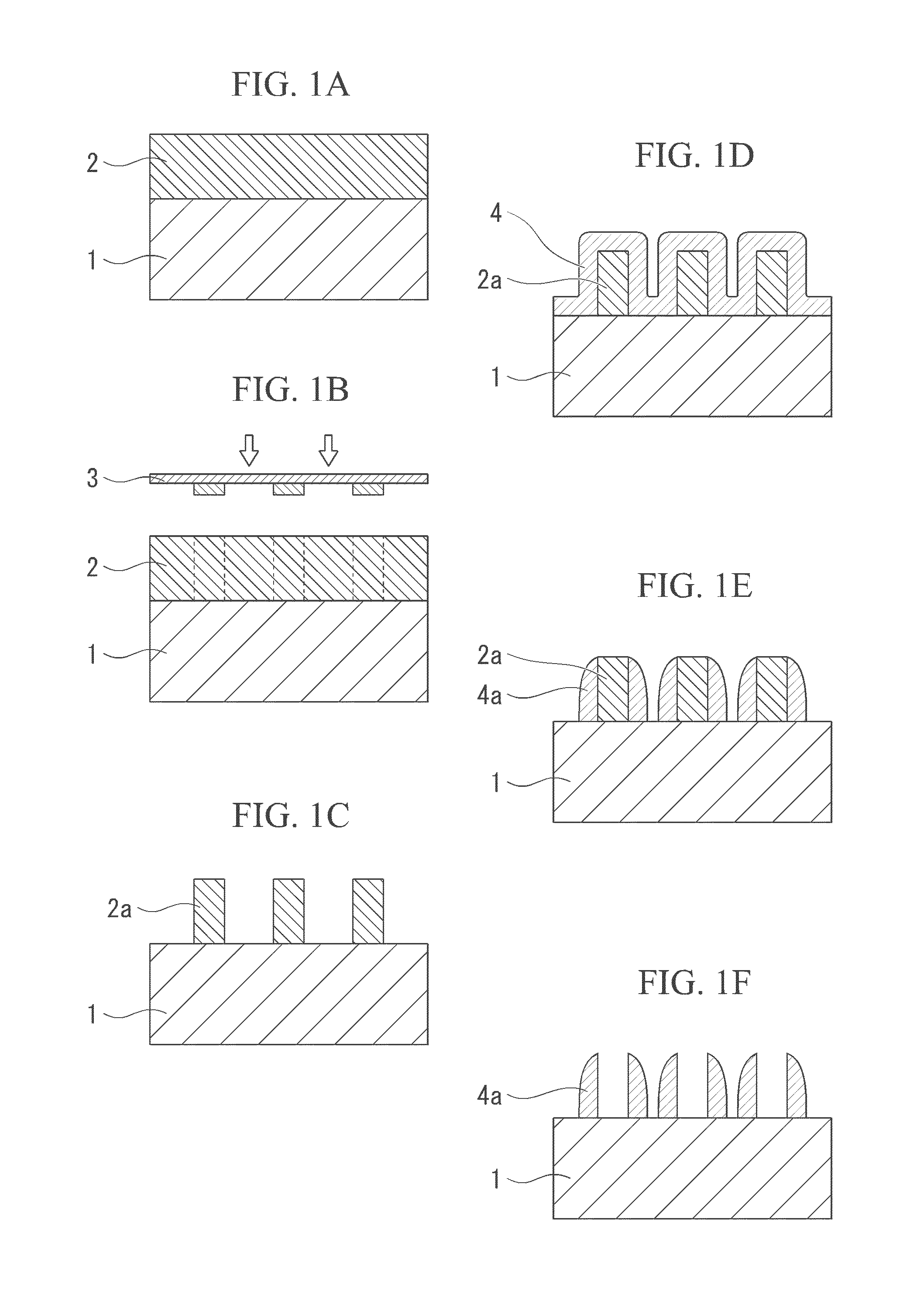
A method of forming a pattern including applying a resist composition to a substrate to form a resist film, and then subjecting the resist film to exposure and development, thereby forming a first pattern containing a resist film; forming a SiO2 film on the surface of the first pattern and the substrate; subjecting the SiO2 to etching such that the SiO2 film remains only on a side wall portion of the first pattern; and removing the first pattern, thereby forming a second pattern containing the SiO2 film. Thr resist composition contains a base component that exhibits changed solubility in a developing solution under action of an acid, and an acid generator component that generates acid upon exposure, the base component containing a resin component containing a structural unit having an acid decomposable group which exhibits increased polarity by the action of acid and has no polycyclic group.
Description
TECHNICAL FIELD[0001]The present invention relates to a method of forming a pattern in which a second pattern composed of an SiO2 film is formed on a first pattern obtained by conducting exposure to a resist film followed by developing the resist film.[0002]Priority is claimed on Japanese Patent Application No. 2012-027462, filed Feb. 10, 2012, the content of which is incorporated herein by reference.BACKGROUND ART[0003]Techniques (pattern-forming techniques) in which a fine pattern is formed on top of a substrate, and a lower layer beneath that pattern is then fabricated by conducting etching with this pattern as a mask are widely used in the production of semiconductor devices and liquid display device. These types of fine patterns are usually formed from an organic material, and are formed, for example, using a lithography method or a nanoimprint method or the like. In lithography techniques, for example, a resist film composed of a resist material containing a base component suc...
Claims
Login to View More Application Information
Patent Timeline
 Patent Type & AuthorityApplications(United States)
IPC IPC(8): G03F7/20
CPCG03F7/2026G03F7/0045G03F7/405G03F7/26H01L21/0273
InventorMOTOIKE, NAOTOOHMORI, KATSUMIHATO, TOSHIAKIYAEGASHI, HIDETAMIOYAMA, KENICHI
OwnerTOKYO OHKA KOGYO CO LTD