Magnetron sputtering device, method for controlling magnetron sputtering device, and film forming method

a magnetron sputtering and film forming technology, applied in vacuum evaporation coatings, electrolysis components, coatings, etc., can solve the problems of special type of abnormal discharge (tracking arc), damage to the thin film, and the film forming speed decreases, so as to improve the quality of the thin film formed on the substrate, the effect of reducing the abnormal discharge voltage in the chamber

Inactive Publication Date: 2013-08-22
SHARP KK
View PDF2 Cites 3 Cited by
  • Summary
  • Abstract
  • Description
  • Claims
  • Application Information

AI Technical Summary

Benefits of technology

[0016]According to the present invention, a prescribed voltage is applied to the target part from the power source while the magnet part is away from the approach points, which are points respectively closest to the side walls of the chamber, and the prescribed voltage is decreased when the magnet part reaches one of the approach points, and thus, even when the magnet part reaches an approach point, it is possible to mitigate abnormal discharge voltage in the chamber. As a result, it is possible to greatly improve the quality of the thin film formed on the substrate.

Problems solved by technology

Factors that inhibit thin film characteristics when forming a film using the sputtering method include damage to the thin film due to high energy particles impacting a substrate.
However, in the magnetron sputtering method, there is a problem that a special type of abnormal discharge (tracking arc) occurs, in which the arc rotates on parts of the target where there are zero components of the magnetic field perpendicular to the target surface (in other words, parts of the target that are etched the most).
As the tracking arc occurs, the discharge impedance changes and power is not supplied efficiently to the target, which results in an undesirable situation in which the film forming speed decreases, or the film is not formed at all.

Method used


Image

  • Magnetron sputtering device, method for controlling magnetron sputtering device, and film forming method
  • Magnetron sputtering device, method for controlling magnetron sputtering device, and film forming method
  • Magnetron sputtering device, method for controlling magnetron sputtering device, and film forming method

Examples


embodiment 1

Effects of Embodiment 1

[0060]Therefore, according to Embodiment 1, when the magnet part 40 is away from approach points, which are points respectively closest to the side walls 51 of the chamber 50, a prescribed voltage is applied to the target part 20 from the power sources 30, but when the magnet part 40 has reached an approach point, the prescribed voltage is lowered, and thus, even when the magnet part 40 has reached an approach point, it is possible to mitigate abnormal discharge voltage in the chamber 50 by appropriately decreasing the discharge voltage. As a result, it is possible to increase the uniformity of the thin film formed on the substrate 10, and to greatly improve the film quality thereof.

Embodiment 2

[0061]FIGS. 9 to 15 show Embodiment 2 of the present invention.

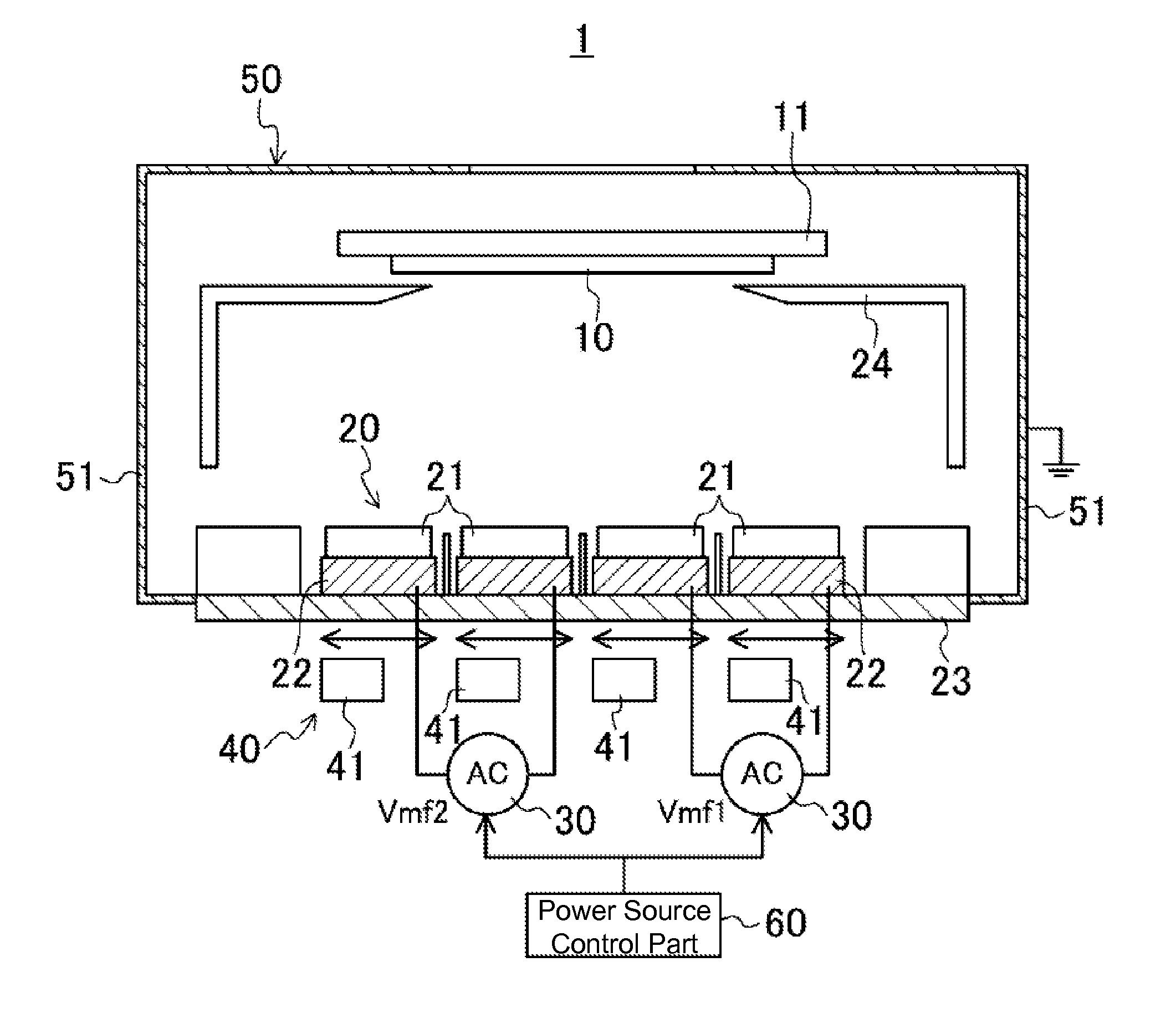
[0062]FIG. 9 is a cross-sectional view that shows a schematic configuration of a magnetron sputtering device 1 of Embodiment 2. FIG. 10 is a plan view that shows a positional relation between a magnet part 4...

embodiment 2

Effects of Embodiment 2

[0084]Therefore, in Embodiment 2, as in Embodiment 1, while a prescribed voltage is applied by the power source 30 to the target part 20 when the magnet part 40 is away from an approach point, the prescribed voltage is lowered when the magnet part 40 reaches an approach point, and thus, even when the magnet part 40 reaches an approach point, it is possible to mitigate abnormal discharge voltage in the chamber 50 by appropriately lowering the discharge voltage. As a result, it is possible to increase the uniformity of the thin film formed on the substrate 10, and to greatly improve the film quality thereof.

embodiment 3

[0085]FIGS. 16 to 18 show Embodiment 3 of the present invention.

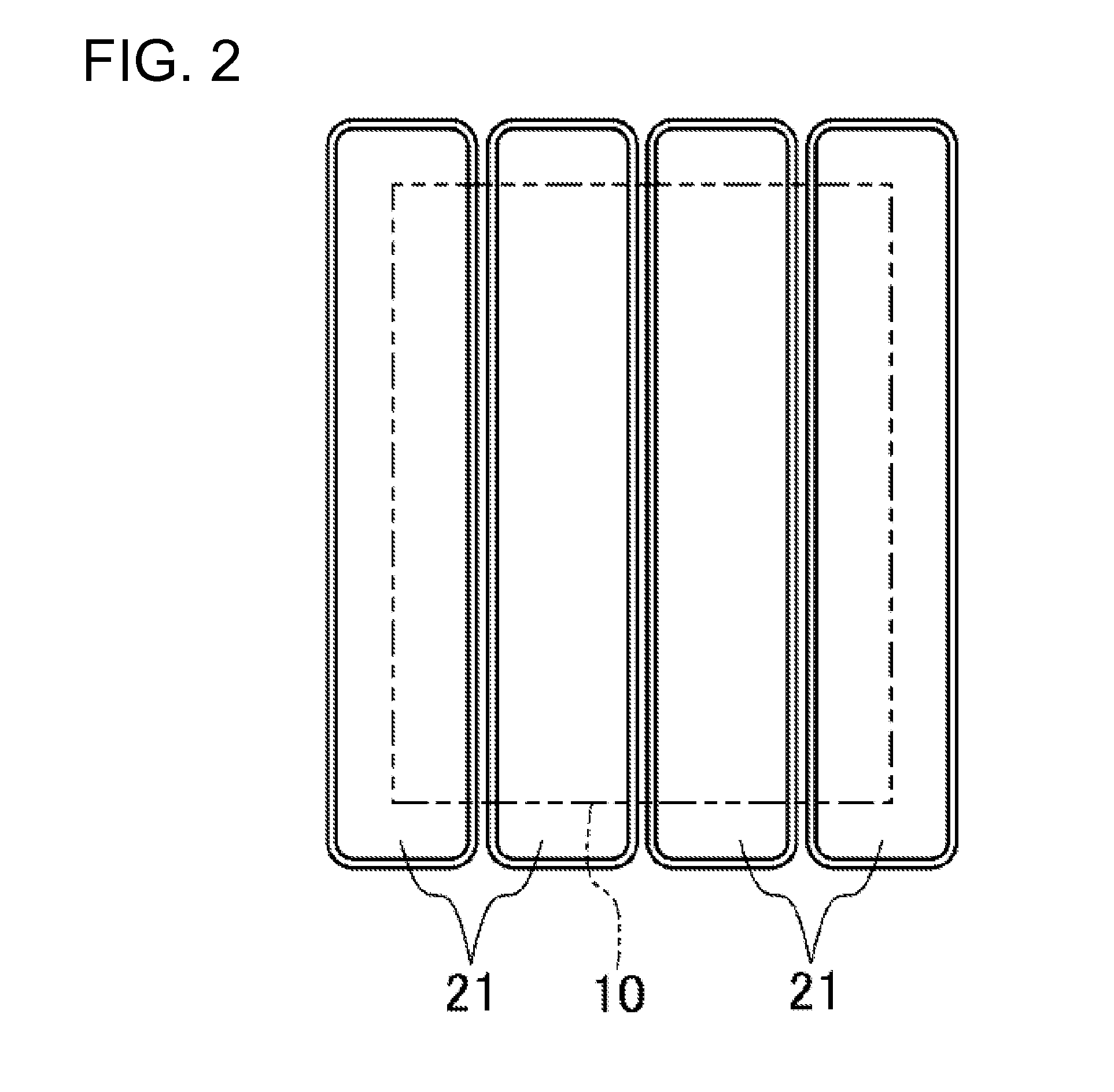
[0086]FIG. 16 is a cross-sectional view that shows a schematic configuration of a magnetron sputtering device 1 of Embodiment 3. FIG. 17 is a plan view that shows a positional relation between a magnet part 40 and a substrate 10 in Embodiment 3. FIG. 18 is a plan view that shows a positional relation between the magnet part 40 and regions of the substrate 10 where defects in film quality have occurred.

[0087]Embodiment 3 is similar to Embodiment 2, except the magnet part 40 is constituted of one magnet 41.

[0088]In other words, as shown in FIG. 16, a magnetron sputtering device 1 of the present embodiment has a substrate holding part 11, substrate masks 24, an insulating member 23, a target part 20, and a target support part 22 inside a chamber 50, as in Embodiment 2.

[0089]The magnet part 40 has one magnet 41, which moves back and forth between one edge and the other edge of the target part 20. The substrate 10 has a vert...


PUM

PropertyMeasurementUnit
horizontal lengthaaaaaaaaaa
frequencyaaaaaaaaaa

Abstract

A magnetron sputtering device is provided with: a target part positioned in such a manner as to face a substrate held by a substrate holding part; a power source that supplies power to the target part; a magnet part that moves back and forth along the rear of the target part; a chamber having side walls that are electrically grounded; and a power source control part that controls the power source in such a manner that, while the magnet part is away from approach points, which are points respectively closest to the side walls, a prescribed voltage is applied to the target part by the power source, but the prescribed voltage is reduced when the magnet part reaches one of the approach points.

Description

TECHNICAL FIELD[0001]The present invention relates to a magnetron sputtering device, a method for controlling the magnetron sputtering device, and a film forming method.BACKGROUND ART[0002]The sputtering method is widely known as a dry process technique indispensable in film forming techniques. The sputtering method is a method for forming films in which a noble gas such as Ar gas is introduced into a vacuum container, and direct current (DC) power or radio frequency (RF) power is supplied to a cathode that includes a target, thus generating a glow discharge. The former is referred to as DC sputtering, and the latter is referred to as RF sputtering.[0003]The sputtering method includes the magnetron sputtering method in which a magnet is disposed on the rear of a target in an electrically grounded chamber, which increases the concentration of plasma in the vicinity of the target surface, thereby allowing film forming to be conducted quickly. The magnetron sputtering method includes t...

Claims


Application Information

Patent Timeline
Patent Type & Authority Applications(United States)
IPC IPC(8): C23C14/35
CPCC23C14/35C23C14/54C23C14/351H01J37/3476H01J37/3455H01J37/3464H01J37/3405
Inventor YOSHIDA, TOKUO
Owner SHARP KK
Why Eureka
Try Eureka