
Apparatus for manufacturing photovoltaic cell

a photovoltaic cell and apparatus technology, applied in the field of photovoltaic cells, can solve the problems of difficult to form a light absorption layer by using such materials, high manufacturing cost, and high manufacturing cos

Inactive Publication Date: 2013-08-29
RES COOPERATION FOUND OF YEUNGNAM UNIV
View PDF17 Cites 4 Cited by
  • Summary
  • Abstract
  • Description
  • Claims
  • Application Information

AI Technical Summary

Benefits of technology

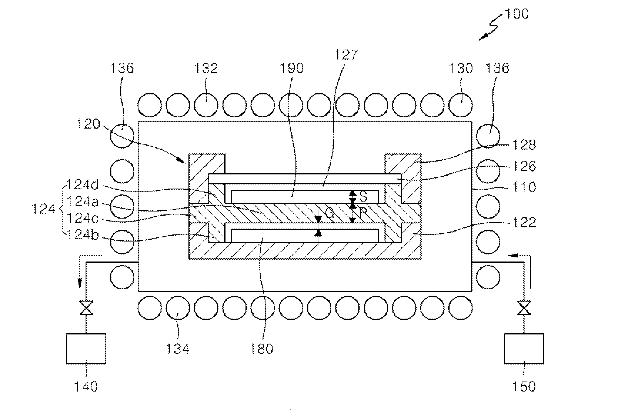
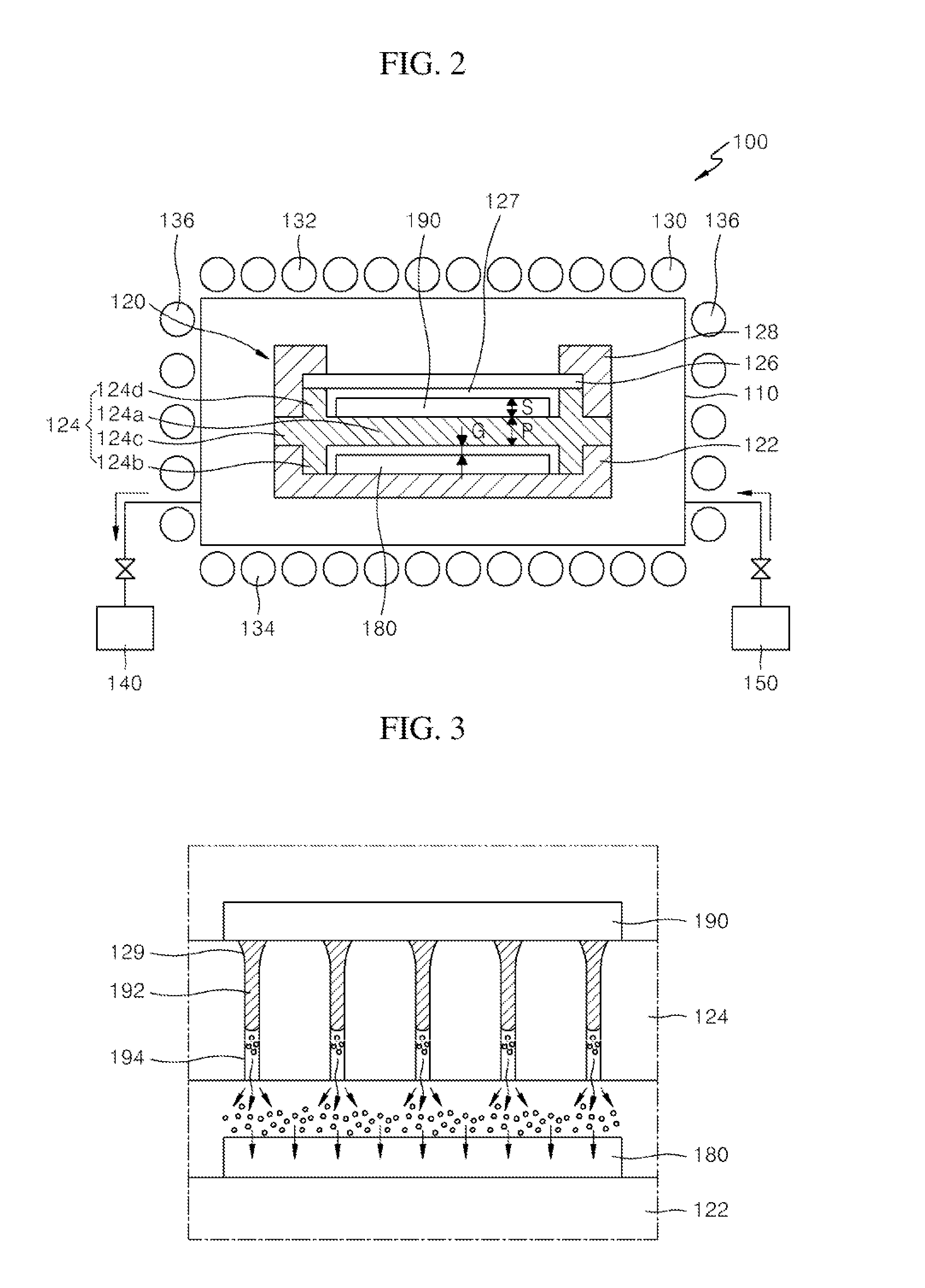
The present invention provides an apparatus for manufacturing a photovoltaic cell by promoting chalcogenation. The apparatus includes a chamber, an object supporting element, and a microporous member with micropores that allow a chalcogen source to reach the object in a fluid path. The microporous member is made of graphite with a specific density and porosity. The micropores have a size that allows a chalcogen liquid to pass through while a chalcogen gas passes through. The apparatus also includes a window element for containing the evaporated portion of the chalcogen source and a fixing element for positioning the window element. The microporous member can be a continuous, monolithic structure or assembled from separate parts. The apparatus can deliver more heat to a lower portion of the chamber than an upper portion and the space between the object and the microporous member is no greater than 1 mm.

Problems solved by technology

However, due to requirements regarding lightweight and thin structures, manufacturing costs, productivity, and production applicability, compound thin film photovoltaic cells, which are second generation photovoltaic cells, are being developed as an alternative.
However, since CIGS and CIGSS are poly-membered compounds, it is difficult to form a light absorption layer by using such materials.
In addition, since a selenization reaction used in the manufacturing process for a light absorption layer requires toxic and corrosive H2Se gas, the selenization needs to be performed with a great deal of caution.
Manufacturing costs may be high due to the need for installation of a special waste processing apparatus.
Thus, the formed light absorption layer may have a heterogeneous selenium concentration gradient, thereby leading to a decrease in chalcogenation and an increase in surface roughness.
Such problems may result in a decrease in efficiency of a photovoltaic cell.

Method used


Image

  • Apparatus for manufacturing photovoltaic cell
  • Apparatus for manufacturing photovoltaic cell
  • Apparatus for manufacturing photovoltaic cell

Examples


Embodiment Construction

[0033]Hereinafter, embodiments of the present invention will be described more fully with reference to the accompanying drawings. The invention may, however, be embodied in many different forms and should not be construed as being limited to the embodiments set forth herein; rather, these embodiments are provided so that this disclosure will be thorough and complete, and will fully convey concepts of the invention to those of ordinary skill in the art. As used herein, the term “and / or” includes any and all combinations of one or more of the associated listed items. Like reference numerals may denote like elements in different drawings. Furthermore, various elements and regions in drawings may be schematically illustrated. Accordingly, the scope of the present invention is not limited by relative sizes or gaps of elements illustrated in the drawings.

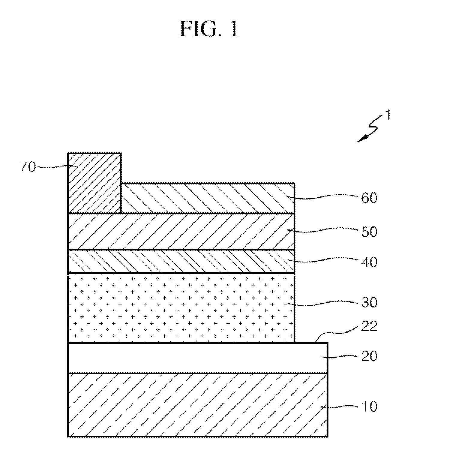
[0034]FIG. 1 is a cross-sectional view of a photovoltaic cell 1 manufactured by using an apparatus for manufacturing a photovoltaic cell...


PUM

PropertyMeasurementUnit
densityaaaaaaaaaa
porosityaaaaaaaaaa
thicknessaaaaaaaaaa

Abstract

Provided is an apparatus for manufacturing a photovoltaic cell in which a light absorption layer is formed by promoting chalcogenation. The apparatus includes a chamber, an object supporting element which is disposed inside the chamber and on which an object is mounted, and a microporous member which is disposed to cover the object supporting element, on which a chalcogen source is mounted, and which has micropores having such a size that the chalcogen source reaches the object through the micropores.

Description

CROSS-REFERENCE TO RELATED PATENT APPLICATIONS[0001]This application claims the benefit of Korean Patent Applications No. 10-2012-0019370, filed on Feb. 24, 2012, and 10-2012-0019371, filed on Feb. 24, 2012, in the Korean Intellectual Property Office, the disclosure of which is incorporated herein in its entirety by reference.BACKGROUND OF THE INVENTION[0002]1. Field of the Invention[0003]Embodiments of the present invention relate to a photovoltaic cell, and in particular, to an apparatus for manufacturing a photovoltaic cell including a chalcogen material and a method for manufacturing a photovoltaic cell including a chalcogen material.[0004]2. Description of the Related Art[0005]Development of alternative energy resources, in particular, solar energy resources, is actively carried out to stave off depletion of petroleum resources. The development of solar energy resources is mainly performed by solar light power generation obtained by converting solar energy into electric energy,...

Claims


Application Information

Patent Timeline
Patent Type & Authority Applications(United States)
IPC IPC(8): H01L31/18
CPCH01L31/18H01L21/02568H01L31/0322H01L31/0749H01L21/02614C23C14/243C23C14/28C23C14/5866Y02E10/541Y02P70/50
Inventor JEON, CHAN-WOOK
Owner RES COOPERATION FOUND OF YEUNGNAM UNIV
Learn More