Display panel
a display panel and display panel technology, applied in non-linear optics, instruments, optics, etc., can solve the problems of difficult to appropriately perform a desired display and tend to display unevenness, and achieve the effect of suppressing display unevenness
- Summary
- Abstract
- Description
- Claims
- Application Information
AI Technical Summary
Benefits of technology
Problems solved by technology
Method used
Image

Examples
embodiment 1
[0063]The display panel according to Embodiment 1 is a liquid crystal display panel including: a pair of substrates between which a space is held by photo spacers; and a liquid crystal layer which is sealed between the pair of substrates. One substrate of the pair of substrates constitutes an active matrix substrate including thin film transistors (TFT: Thin Film Transistor), gate bus lines (scanning lines), source bus lines (signal lines), pixel electrodes, interlayer insulation films that electrically isolates the various lines and electrodes, and an alignment film which gives an orientation to the liquid crystal molecules. The other substrate of the pair of substrates constitutes a color filter substrate including color filters, a black matrix, a common electrode, and an alignment film which gives an orientation to the liquid crystal molecules.
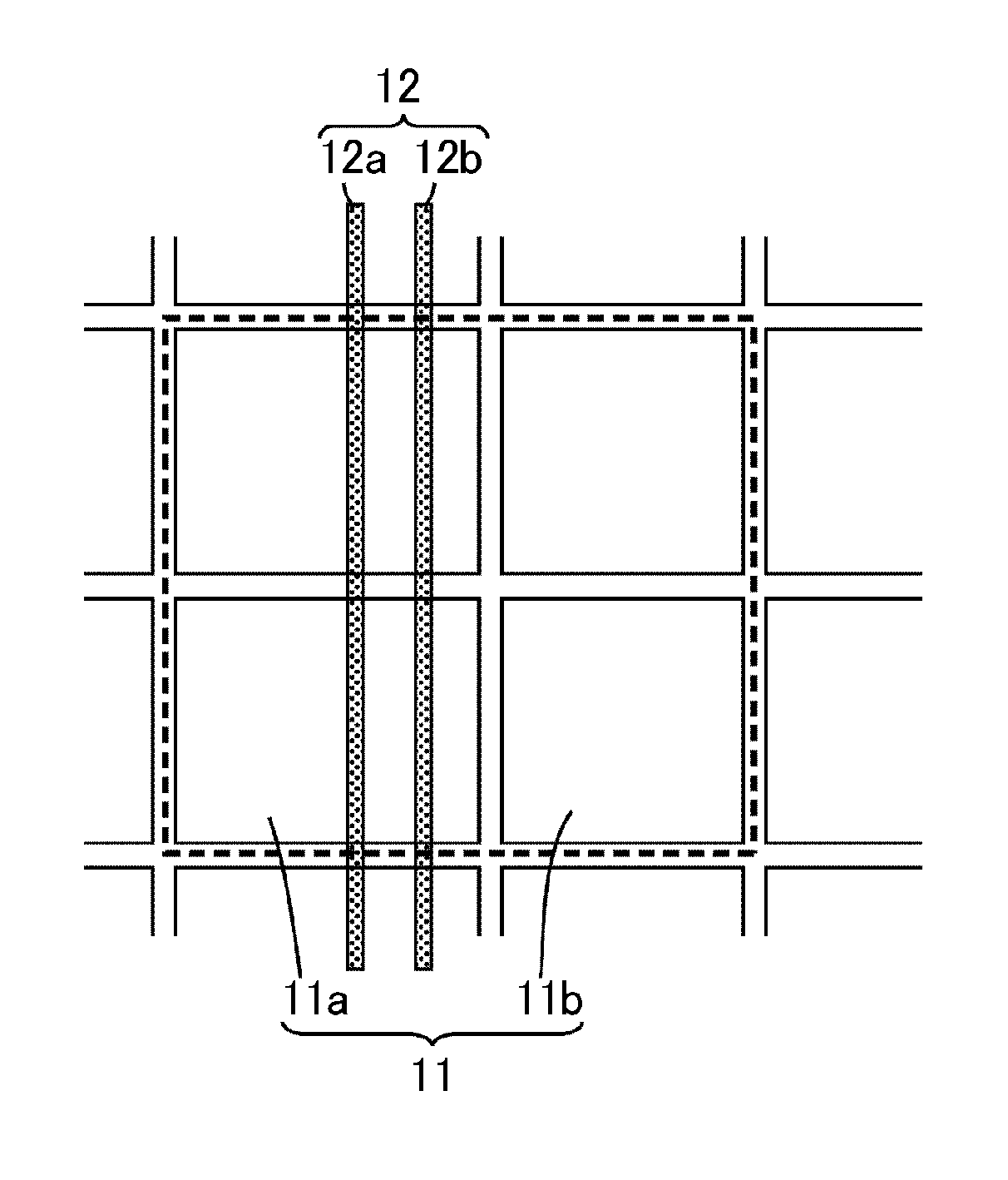
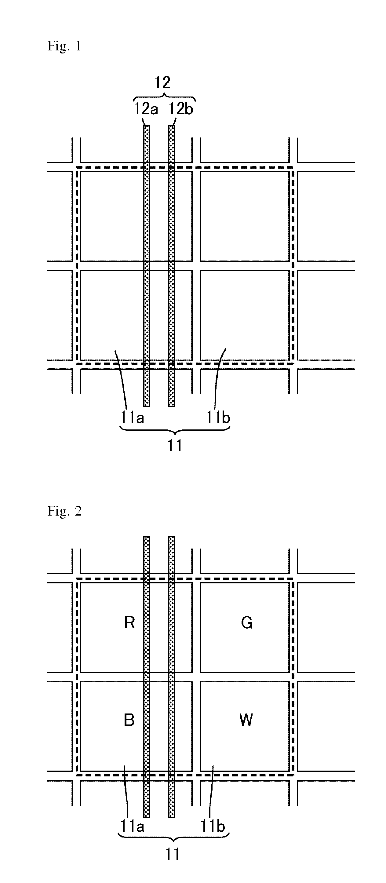
[0064]The pixel electrodes are arranged in matrix. Each region, in which each pixel electrode is positioned, corresponds to one picture el...
embodiment 2
[0092]A display panel according to Embodiment 2 is the same as the display panel according to Embodiment 1 except that the source bus lines, the TFTs, and the spacers are differently positioned.
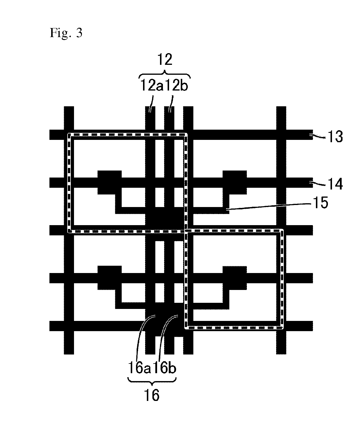
[0093]FIG. 6 is a schematic plan view illustrating a wiring structure of the active matrix substrate of the display panel according to Embodiment 2. As shown in FIG. 6, pixel electrodes 11 are arranged in matrix, and source bus lines 12, through which image signals are sent to pixel electrodes 11, linearly extend in the column direction. A single pixel is a region (the portion surrounded by the dotted line of FIG. 6) in which four pixel electrodes 11 arranged in a squared shape are positioned, and two types (2n total) of large and small pixel electrodes 11 are disposed in the single pixel.
[0094]In Embodiment 2, the gap between the source bus lines 12 is increased compared with the case of Embodiment 1. As described above, the entireties of the source bus lines 12 in the widthwise direction of...
embodiment 3
[0100]A display panel according to Embodiment 3 is the same as the display panel according to Embodiment 1 except that each pixel electrode is not rectangular and has a shape of a rectangle partially cut out.
[0101]FIG. 9 is a schematic plan view illustrating a wiring structure of the active matrix substrate of the display panel according to Embodiment 3. As shown in FIG. 9, pixel electrodes 11 are arranged in matrix, and source bus lines 12, through which image signals are sent to pixel electrodes 11, linearly extend in the column direction. A single pixel is a region (the portion surrounded by the dotted line of FIG. 9) in which four pixel electrodes 11 arranged in a squared shape are positioned, and two types (2n total) of large and small pixel electrodes 11 are disposed in the single pixel.
[0102]In Embodiment 3, each of the pixel electrodes 11a having the larger areas among the pixel electrodes 11 is partially cut out. Specifically, the lower side and the right side (the side clo...
PUM
| Property | Measurement | Unit |
|---|---|---|
| colors | aaaaa | aaaaa |
| area | aaaaa | aaaaa |
| electric potential | aaaaa | aaaaa |
Abstract
Description
Claims
Application Information
 - R&D
- Intellectual Property
- Life Sciences
- Materials
- Tech Scout
- Unparalleled Data Quality
- Higher Quality Content
- 60% Fewer Hallucinations
Browse by: Latest US Patents, China's latest patents, Technical Efficacy Thesaurus, Application Domain, Technology Topic, Popular Technical Reports.
© 2025 PatSnap. All rights reserved.Legal|Privacy policy|Modern Slavery Act Transparency Statement|Sitemap|About US| Contact US: help@patsnap.com